
System and method for providing a power bus in a wirebond leadframe package

a technology of wirebond leadframe and power bus, which is applied in the direction of electrical equipment, semiconductor devices, semiconductor/solid-state device details, etc., can solve the problems of increasing the size and weight of the package, increasing the cost and complexity, etc., and achieving the effect of maximizing the number of die bondpads

Inactive Publication Date: 2009-02-24
MARVELL INT TECH
View PDF1 Cites 2 Cited by
  • Summary
  • Abstract
  • Description
  • Claims
  • Application Information

AI Technical Summary

Benefits of technology

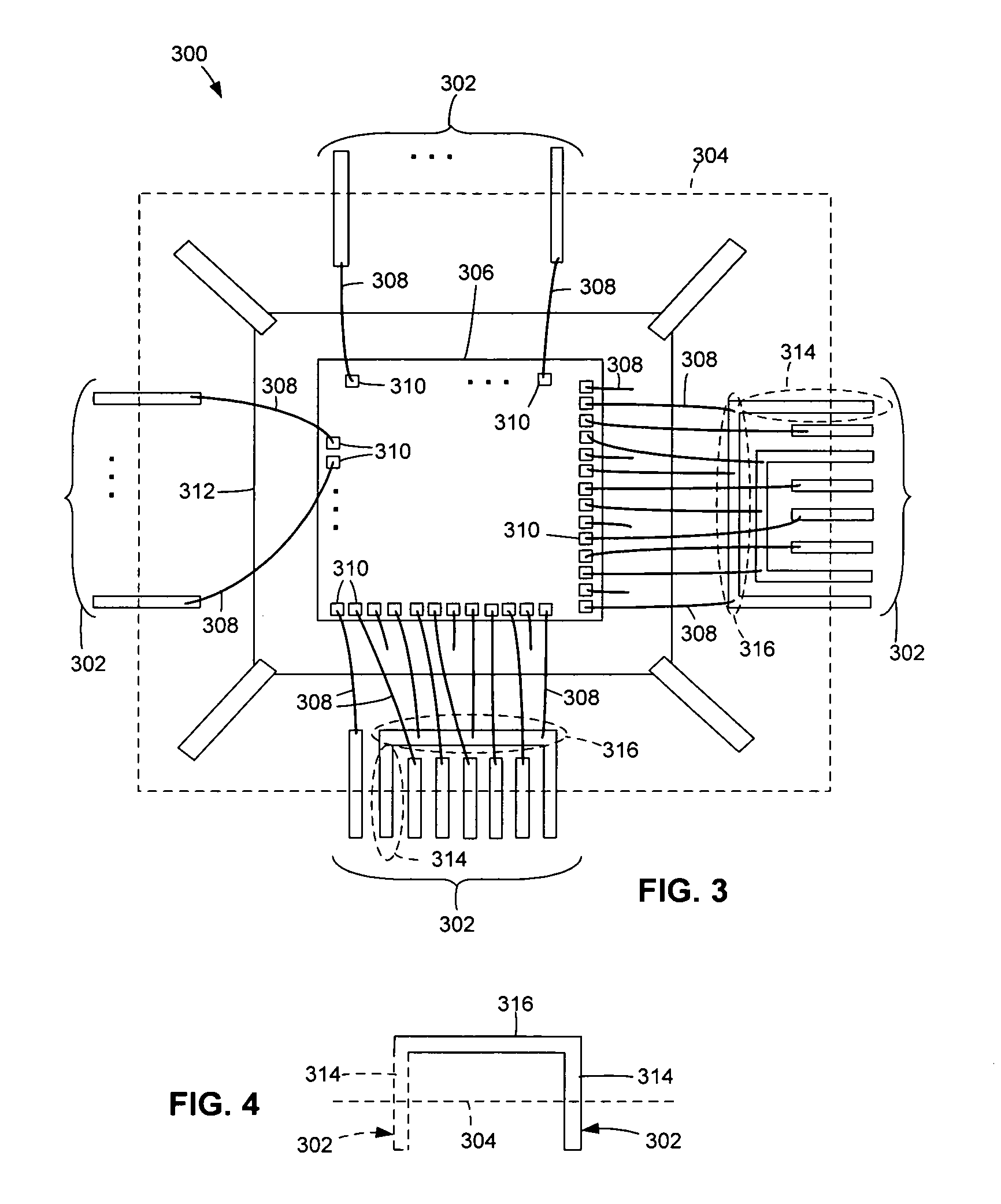
"The present invention relates to an integrated circuit package with leads that have an extended shape, allowing for more than one bondwire to be attached to it. This design allows for efficient connection of bondwires from different die bondpads, resulting in a bus-like connection. The elongated lead tips can also interconnect two or more leads, creating a loop-like lead structure. The lead tips can accommodate more die bondpads than conventional QFP packages. The technical effects of this design include improved efficiency and reliability of bonding and reduced size and cost of the integrated circuit package."

Problems solved by technology

Such structures add significant manufacturing cost and increase the size and weight of the package.
The more leads in a QFP package, the greater its size, weight, cost and complexity.
In such an instance, a larger, more complex, less economical package must be selected.

Method used


Image

  • System and method for providing a power bus in a wirebond leadframe package
  • System and method for providing a power bus in a wirebond leadframe package
  • System and method for providing a power bus in a wirebond leadframe package

Examples


Embodiment Construction

[0017]In the following description, like reference numerals indicate like components to enhance the understanding of the invention through the description of the drawings. The drawing figures are not to scale. Also, although specific features, configurations, arrangements and steps are discussed below, it should be understood that such specificity is for illustrative purposes only. A person skilled in the relevant art will recognize that other features, configurations, arrangements and steps are useful without departing from the spirit and scope of the invention.

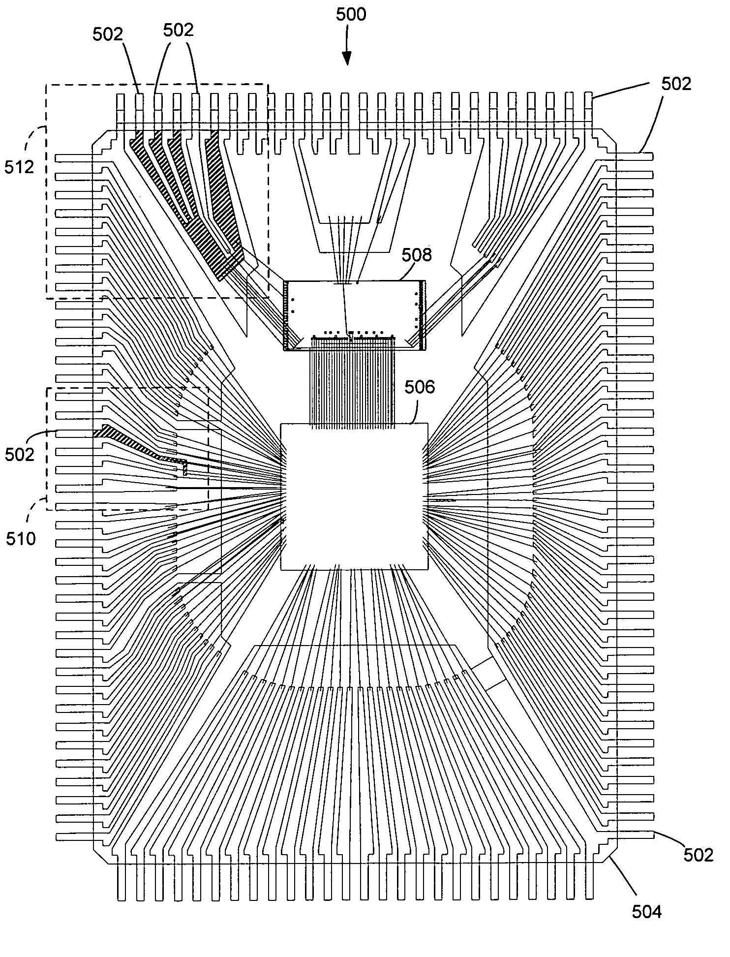
[0018]As illustrated in FIG. 3, in an exemplary embodiment of the present invention, a Quad Flat Pack (QFP) package 300 has four sides with leads 302 extending from the component body 304 (shown in dashed line in this interior view) on all four sides. The electrical connections between the die 306 and the leads 302 of the package are made by wirebonding with bondwires 308. (Some leads 302 and other grouped elements are not s...


PUM


Abstract

An integrated circuit (IC) package, such as a Quad Flat Pack (QFP), has at least one lead with a tip that extends substantially perpendicular to the ends of two or more bondwires, so that there is room for more than one bondwire to be attached to it along its length. Thus, bondwires leading from die bondpads that are not adjacent to one another can be efficiently connected to the same lead in a bus-like manner.

Description

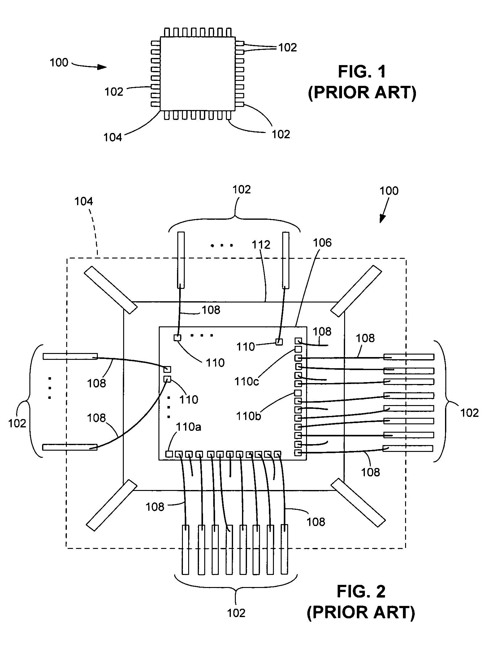
BACKGROUND OF THE INVENTION[0001]Electronic packaging is essentially the final step in the process of fabricating an integrated circuit (IC) or “chip.” In the packaging step, the semiconductor die is mounted on a leadframe, and electrical connections are made between the die and the leads of the leadframe, before encapsulating the assembly in the component body. The leadframe is typically made from a thin sheet of metal by stamping or etching. The majority of IC packages use a method known as wirebonding to make the electrical connections between the die and the leads. In wirebonding, one end of a very fine gold or aluminum bondwire (on the order of 10-100 micrometers in diameter) is attached to a bondpad on the die, and the other end is attached to an end of a lead. The end of the lead to which the bondwire is attached is sometimes referred to as a bondfinger and sometimes as a lead tip. The bondwire ends are typically attached by applying some combination of pressure and heat. The...

Claims


Application Information

Patent Timeline
Patent Type & Authority Patents(United States)
IPC IPC(8): H01L23/495
CPCH01L23/49541H01L24/49H01L24/45H01L2224/45015H01L2224/45124H01L2224/45144H01L2224/48091H01L2224/48137H01L2224/48247H01L2224/49113H01L2224/49171H01L2224/49175H01L2924/01013H01L2924/01079H01L2924/01082H01L2924/14H01L2924/1433H01L2924/20751H01L2924/20752H01L2924/20753H01L2924/20754H01L2924/20755H01L2924/20756H01L2924/20757H01L2924/20758H01L2924/20759H01L2924/00014H01L24/48H01L2224/48257H01L2924/01006H01L2924/01033H01L2924/014H01L2224/48253H01L2924/00H01L2224/05554H01L2924/181H01L2924/00012
Inventor CUSACK, MICHAEL DAVID
Owner MARVELL INT TECH
Learn More