
Surface inspection method and surface inspection apparatus

a surface inspection and surface technology, applied in the direction of mechanical measurement arrangements, mechanical roughness/irregularity measurements, instruments, etc., can solve the problems of typical worse time response characteristic of the photomultiplier tube, existing crystal defects, rough surface of the substrate, etc., to eliminate or reduce its influence

Active Publication Date: 2009-02-03
HITACHI HIGH-TECH CORP
View PDF3 Cites 12 Cited by
  • Summary
  • Abstract
  • Description
  • Claims
  • Application Information

AI Technical Summary

Benefits of technology

This approach effectively reduces the noise caused by the ripple component, enhancing the detection sensitivity for minute contaminants and defects on semiconductor substrates by accurately integrating the scattered light pulses and eliminating residual noise in the signal.

Problems solved by technology

As for the inspection of the substrate surface, crystal defects existing in a shallow region near the substrate surface and surface roughness of the substrate surface also become subjects of the inspection, besides the above-described contaminant particles and defects.
When using such a pulse laser in order to achieve the higher sensitivity, the following problem occurs.
However, the time response characteristic of the photomultiplier tube is typically worse than the time width at half maximum of the pulse laser.
However, the bandwidth of the amplifier is not wide enough to completely integrate and remove the original pulse trains.
It is apparent that the ripple component causes noise in the scattered light intensity signal.

Method used


Image

  • Surface inspection method and surface inspection apparatus
  • Surface inspection method and surface inspection apparatus
  • Surface inspection method and surface inspection apparatus

Examples


Embodiment Construction

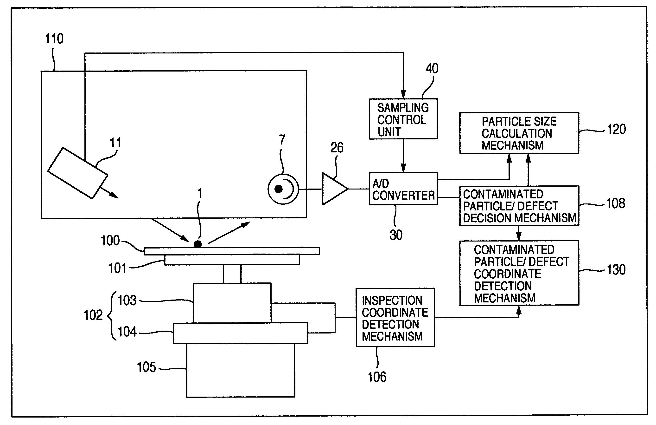
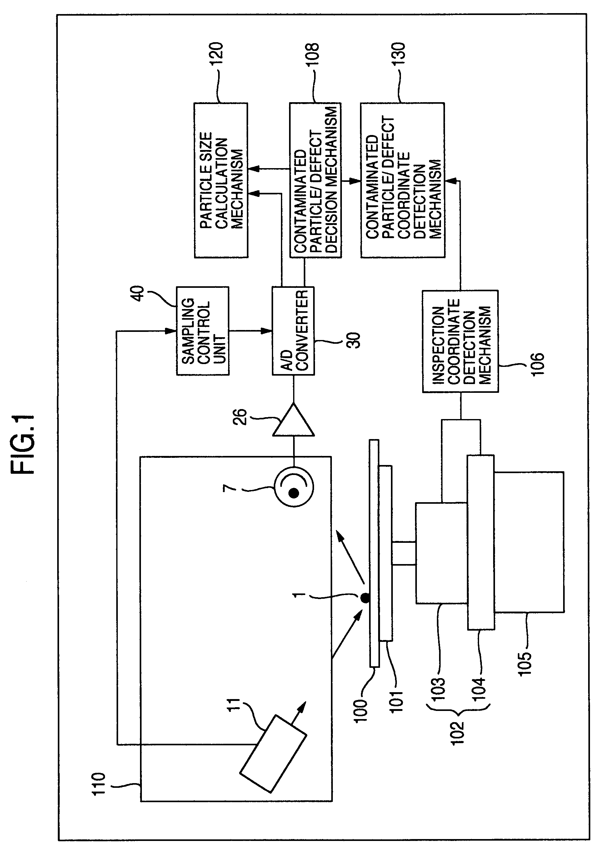
[0038]The present invention relates to a technique for detecting a minute contaminated particle or defect when it is present on, for example, a semiconductor substrate (semiconductor wafer), and a technique for measuring information concerning surface roughness of the substrate. In particular, the present invention relates to a surface inspection technique for inspecting the substrate surface by using a pulse laser, which performs pulse oscillation repetitively in time, as the light source.

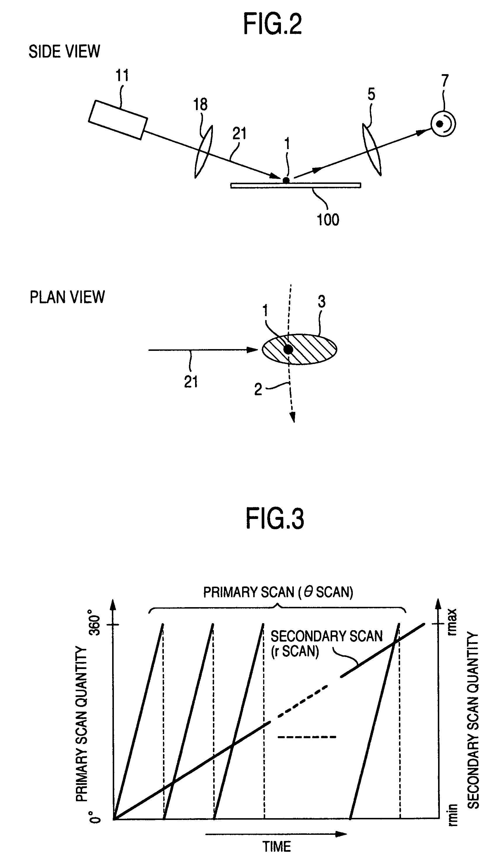
[0039]A surface inspection apparatus according to an embodiment of the present invention includes an object to be inspected moving stage, a pulse laser light source, illumination means for irradiating an illumination region having a predetermined size on the surface of an object to be inspected with laser light emitted from the pulse laser light source, scattered / diffracted / reflected light collecting means for collecting light generated by scattering / diffracting / reflecting the irradiated light in ...


PUM

PropertyMeasurementUnit
wavelengthaaaaaaaaaa
oscillation wavelengthaaaaaaaaaa
frequencyaaaaaaaaaa

Abstract

When detecting light scattered by an object to be inspected by using a pulse laser as a light source, noise increases unless a sampling repletion period of an A / D converter is determined so as to be related to a pulse oscillation repetition period of the light source. (1) The sampling repletion period of the A / D converter is set equal to the pulse oscillation repetition period of the light source or an integer times thereof, and the sampling is synchronized with oscillation of the light source. Or (2) the sampling repletion period of the A / D converter is set equal to a half-integer times the pulse oscillation repetition period of the light source. Even if a ripple component resulting from emission pulses of the light source remains in the scattered light signal supplied to the A / D converter remains, therefore, its influence can be eliminated or reduced.

Description

BACKGROUND OF THE INVENTION[0001]The present invention relates to a surface inspection method and a surface inspection apparatus.[0002]Conventionally, on a production line for a semiconductor substrates (semiconductor wafer), defects such as contaminant particles which have adhered to the surface of the substrate or scratches generated during working are inspected to monitor the dust generating situation of a production apparatus. For example, in the semiconductor substrate before circuit pattern forming, it is necessary to detect minute contaminant particles and defects as small as several nm or less on the surface. As for the inspection of the substrate surface, crystal defects existing in a shallow region near the substrate surface and surface roughness of the substrate surface also become subjects of the inspection, besides the above-described contaminant particles and defects. A technique for detecting minute defects on the surface of an object to be inspected such as a semicon...

Claims


Application Information

Patent Timeline
Patent Type & Authority Patents(United States)
IPC IPC(8): G01N21/88
CPCG01N21/47G01N21/9501
Inventor MATSUI, SHIGERU
Owner HITACHI HIGH-TECH CORP
Learn More