Taking optical system

an optical system and optical system technology, applied in the field of taking optical systems, can solve the problems of increasing the number of lens elements and the total length, increasing the cost, and increasing the number of components, and achieves the effects of slim and compact, wide angle of view, and high definition

Inactive Publication Date: 2009-01-27
KONICA MINOLTA OPTO
View PDF3 Cites 4 Cited by
  • Summary
  • Abstract
  • Description
  • Claims
  • Application Information

AI Technical Summary

Benefits of technology

[0010]In view of the conventionally encountered inconveniences mentioned above, it is an object of the present invention to provide a taking optical system that, despite being inexpensive and slim, offers performance so high that higher definition and wider angles of view can be coped with.
[0014]Thus, according to the present invention, it is possible to provide a taking optical system that, despite being inexpensive and extremely slim, offers performance so high that higher definition and wider angles of view can be coped with. By employing a taking optical system according to the present invention in a device such as a digital camera, cellular phone, or personal digital assistant, it is possible to make the device high-performance, versatile, slim and compact, low-cost, and otherwise improved.

Problems solved by technology

Seeking larger image sizes and higher resolution in this type of optical system, however, leads to an increased number of lens elements and an increased total length.
The taking optical system disclosed in Patent Publication 1 uses two prisms, resulting in high cost.
Moreover, an aperture stop is disposed between the two prisms, increasing the number of components and thus further increasing the cost.
Furthermore, inaccurately positioning the aperture stop leads to poor optical performance.
However, although slimness is achieved to some extent, higher definition and wider angles of view cannot satisfactorily be coped with.
Specifically, unless the prism is properly designed and arranged, it is not possible to achieve satisfactory slimness, nor to obtain high performance.

Method used


Image

  • Taking optical system
  • Taking optical system
  • Taking optical system

Examples


examples

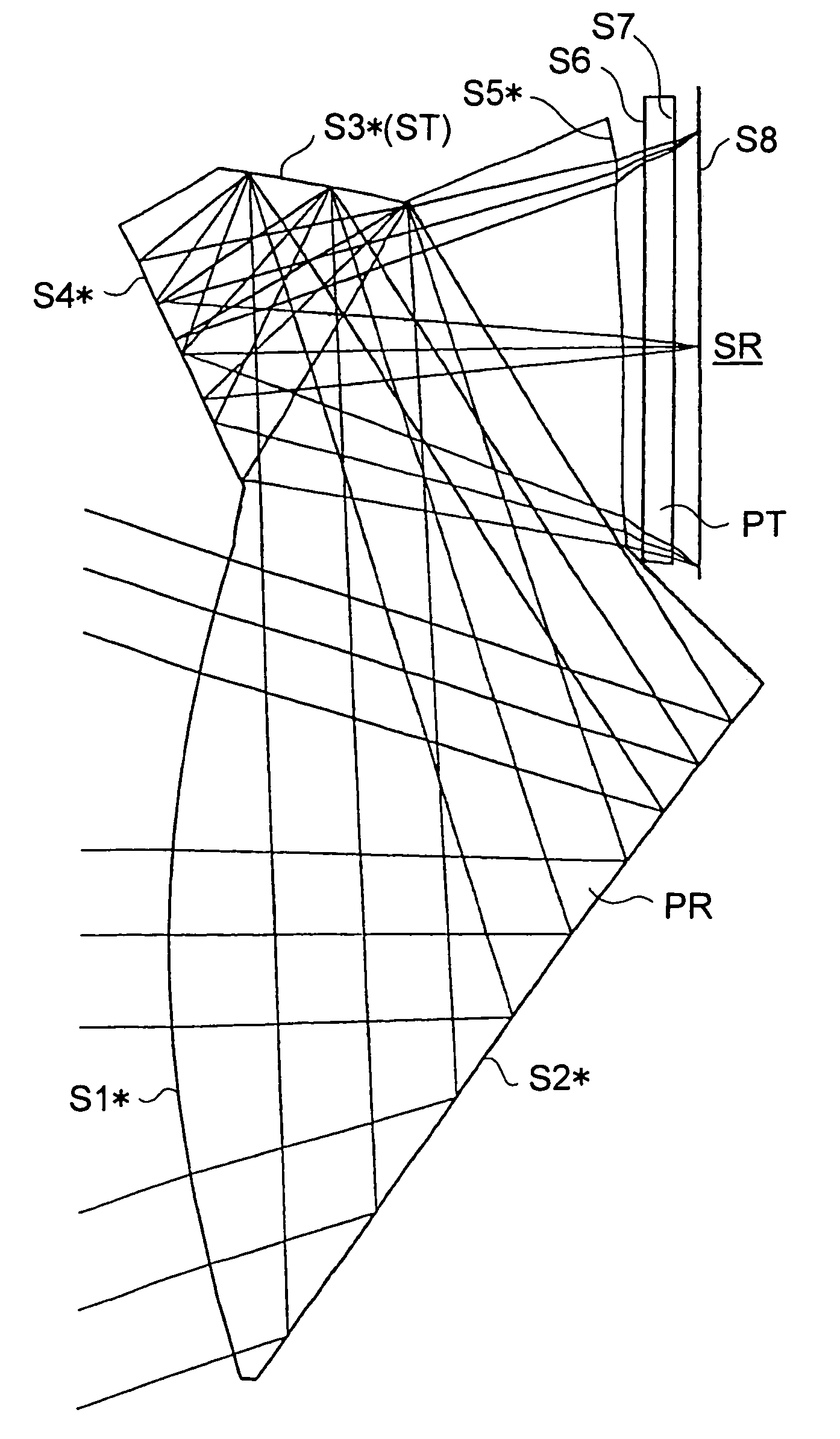
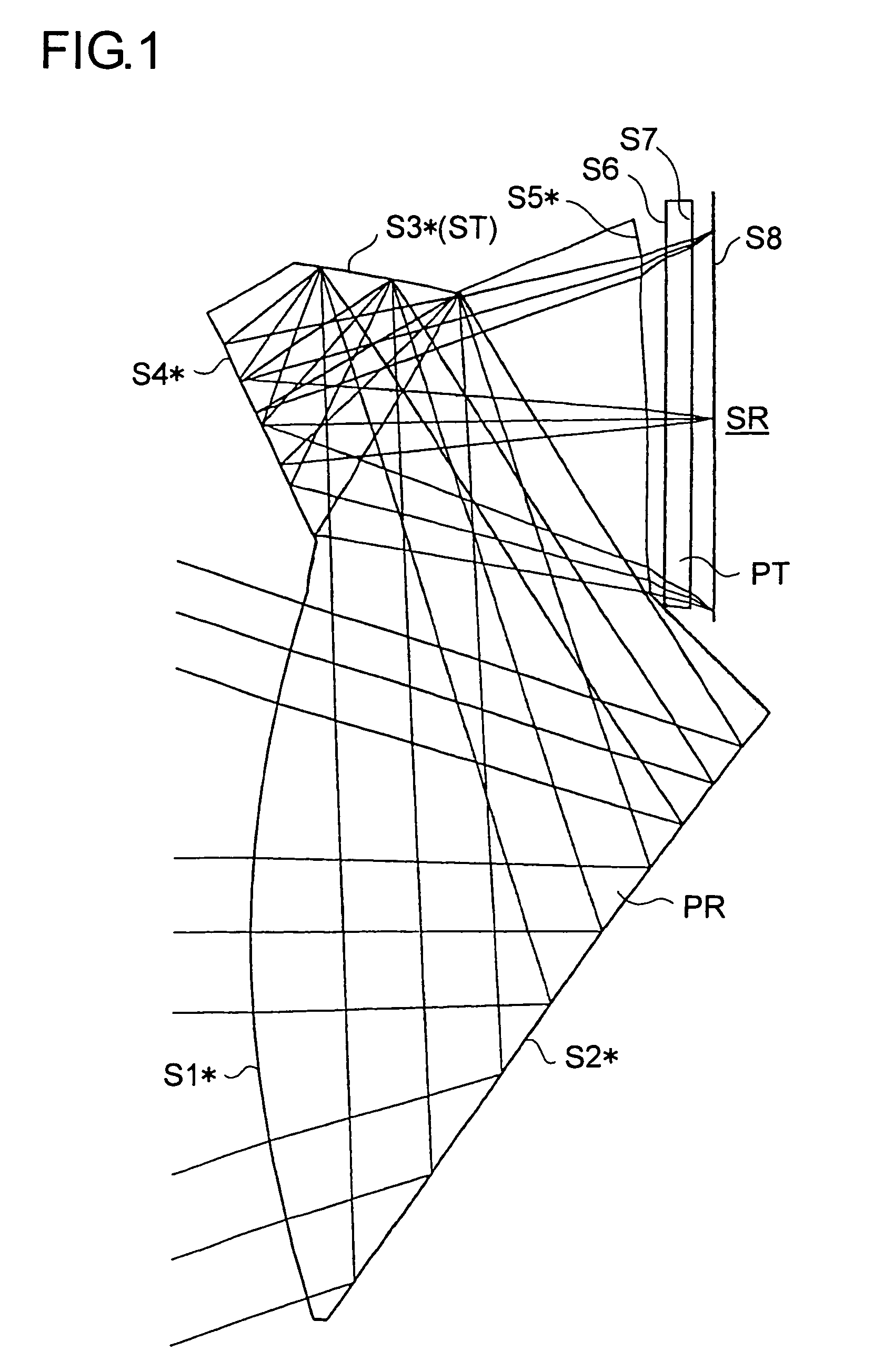
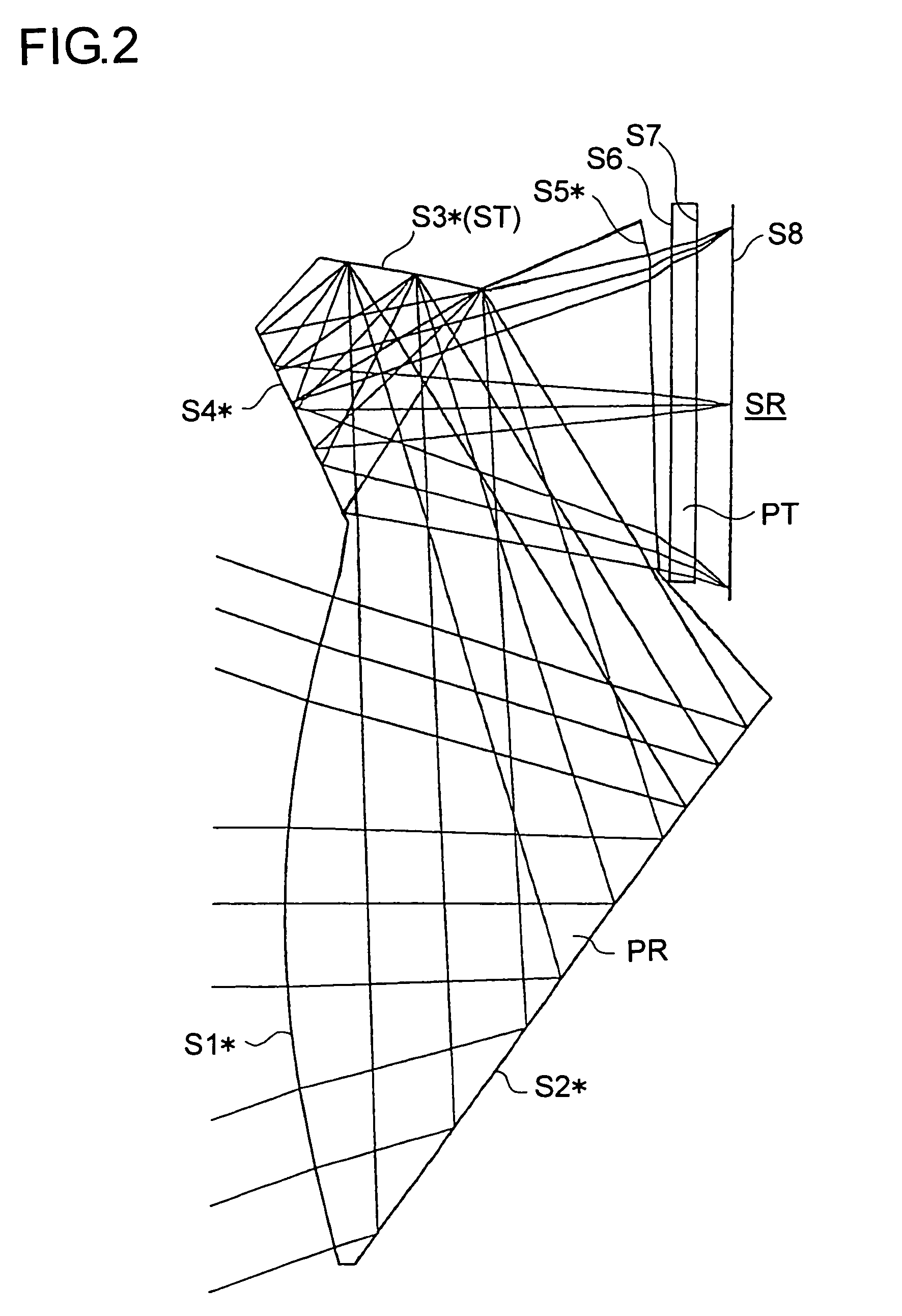
[0464]Hereinafter, numerical examples of taking optical systems embodying the present invention will be presented with reference to their construction data and other data. Examples 1 to 3 presented below are numerical examples corresponding to the first to third embodiments, respectively, described above. Thus, the optical path diagrams (FIGS. 1 to 3) showing the first to third embodiments also show the optical constructions and other features of Examples 1 to 3, respectively.

[0465]Tables 1 to 3, Tables 4 to 6, and Tables 7 to 9 show the construction data of Examples 1 to 3, respectively. In the basic construction data shown in Tables 1, 4, and 7 (where i represents the surface number), Si (i=1, 2, 3, . . . ) represents the i-th surface as counted from the object side, ri (i=1, 2, 3, . . . ) represents the radius of curvature (mm) of the surface Si, and Ni and vi represent the refractive index (Nd) for the d-line and the Abbe number (vd) of the optical material filling the axial dis...


PUM


Abstract

A taking optical system for forming an optical image of an object on the light-receiving surface of an image sensor has at least one optical prism that has an entrance surface, at least three reflective surfaces each curved, and an exit surface, and that receives rays from the object side through the entrance surface, then reflects the rays on the at least three reflective surfaces, and then lets out the rays through the exit surface. The optical prism is formed of a medium having a refractive index of 1.2 or more. An optical aperture is disposed on or near one of the at least three reflective surfaces. At least one of the at least three reflective surfaces is an eccentrically disposed rotation-asymmetric surface. Let the ray traveling from the center of the object through the center of the optical aperture to the center of the image surface be called a base ray, then the intersections of the base ray with the entrance surface, each of the reflective surfaces, and the exit surface all lie approximately on the same plane.

Description

[0001]This application is based on Japanese Patent Application No. 2005-78867 filed on Mar. 18, 2005, Japanese Patent Application No. 2005-78918 filed on Mar. 18, 2005, and Japanese Patent Application No. 2005-80907 filed on Mar. 22, 2005, the contents of which are hereby incorporated by reference.BACKGROUND OF THE INVENTION[0002]1. Field of the Invention[0003]The present invention relates to a taking optical system, and more particularly to a slim taking optical system suitable for use in a digital device equipped with an image input capability so as to be capable of capturing an image of a subject by means of an image sensor.[0004]2. Description of Related Art[0005]In recent years, more and more cellular phones and personal digital assistants (PDAs) have been becoming equipped with a digital still camera or digital video unit for capturing images. These digital devices are required to be compact so as to be easily portable, and are simultaneously required to capture images with hi...

Claims


Application Information

Patent Timeline
Patent Type & Authority Patents(United States)
IPC IPC(8): G02B5/04
CPCG02B13/001G02B13/002G02B13/007G02B17/086
Inventor SHIMO, MITSUAKI
Owner KONICA MINOLTA OPTO
Why Eureka
Try Eureka