
Apparatuses and methods for forming electronic assemblies

a technology of electronic assemblies and apparatus, applied in the field of microelectronic assemblies, can solve the problems of inapplicability generally not applicable to very small or numerous elements, and generally not providing a high-quality display, so as to minimize the chances of security breaches

Inactive Publication Date: 2008-08-26
RUIZHANG TECH LTD CO
View PDF15 Cites 61 Cited by
  • Summary
  • Abstract
  • Description
  • Claims
  • Application Information

AI Technical Summary

Benefits of technology

This approach reduces production costs and enhances efficiency by using flexible substrates and a single I / O lead for data transfer, minimizing security risks and enabling flexible smart card designs with improved manufacturing processes.

Problems solved by technology

However, passive matrices generally provide a lower quality display compared to active matrices.
Pick and place methods generally place devices one at a time and are generally not applicable to very small or numerous elements such as those needed for large arrays, such as an active matrix liquid crystal display.
There are disadvantages inherent to the related art.
This process is time consuming and laborious.
Additionally, smart cards are typically manufactured using a batch process which is not efficient.

Method used


Image

  • Apparatuses and methods for forming electronic assemblies
  • Apparatuses and methods for forming electronic assemblies
  • Apparatuses and methods for forming electronic assemblies

Examples


Embodiment Construction

[0049]One embodiment of the invention relates to a contact smart card having a single input / output that is inserted directly into a device and data is transferred through the single input / output of the contact smart card.

[0050]Additionally, blocks having integrated circuits are placed onto a substrate for forming a contact, contactless, or dual smart card which provides a distributed intelligence.

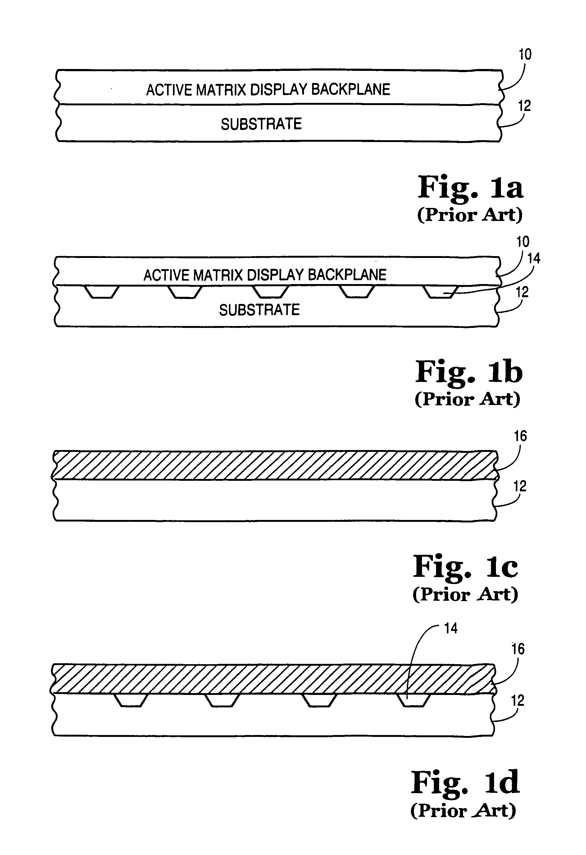
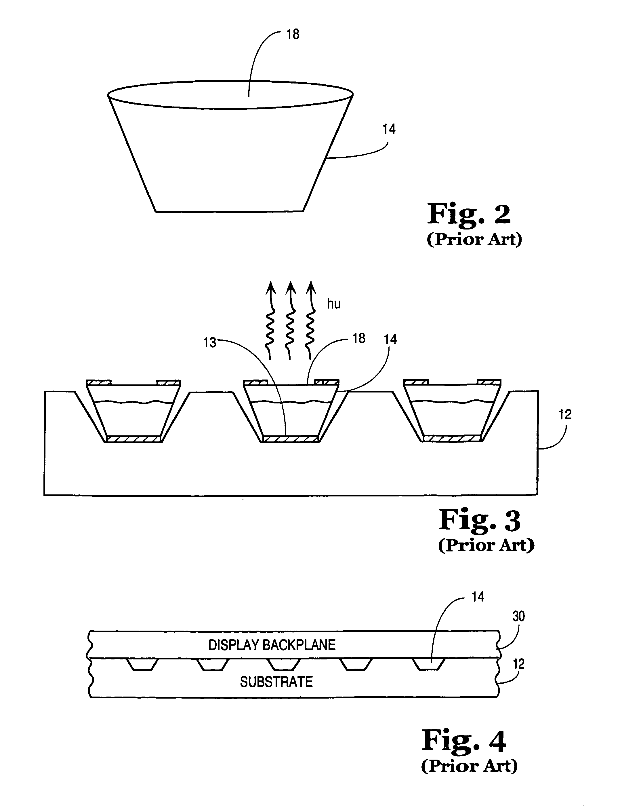
[0051]By fabricating a flexible smart card using fluidic self assembly (FSA) described in U.S. Pat. No. 5,545,291, the cost of producing the smart card is reduced. The smart card has a smart card chip that contacts the display. The smart card also has a molded display cavity with a power, ground, single input / output interconnect formed in the backside of the display. This device may then receive signals and update data that is displayed.

[0052]The backplane of the display may be comprised of a plurality of blocks in which each block has a circuit element thereon. The blocks are contained in ...


PUM


Abstract

Apparatuses and methods for forming microelectronic assemblies are claimed. One embodiment of the invention includes a contact smart card wherein fluidic self assembly is used to build the microelectronic structures on the microelectronic assembly such that a contact smart data is transmitted unidirectionally. A contact smart card is inserted directly into a device that transfers data to a microelectronic assembly coupled to the smart card. Another embodiment of the invention relates to a contactless smart card in which fluidic self assembly is also used here to build the microelectronic assembly. Data is transmitted to an antenna that is embedded in the contactless card in which a plurality of blocks were deposited thereon.

Description

RELATED APPLICATIONS[0001]This is a continuation of application Ser. No. 09 / 932,515, now U.S. Pat. No. 6,863,219, filed on Aug. 17, 2001.BACKGROUND[0002]1. Field of the Invention[0003]This invention relates generally to a microelectronic assembly such as a smart card that includes an integrated circuit component. More particularly, the present invention relates to apparatuses and methods for forming displays coupled to a flexible card in which the display is configurable and alterable based upon data that is received from a signal that contains at least a single stream of serial data.[0004]2. Description of Related Art[0005]Microelectronic assemblies typically include integrated circuit components attached to substrates. Electrical interconnections are formed that allow communication between the integrated circuit component and the substrate for sending and receiving signals for processing. One type of a microelectronic assembly is a “smart card” assembly.[0006]“Smart card” assembli...

Claims


Application Information

Patent Timeline
Patent Type & Authority Patents(United States)
IPC IPC(8): H01L23/02G06K19/077
CPCG06K19/077G06K19/07703H01L2224/95085H01L2924/01079H01L2924/13091H01L2924/1461H01L2924/12041H01L2924/00H01L2924/12044H01L2924/15153H01L2224/95101
Inventor JACOBSEN, JEFFREY JAYSTEWART, ROGER GREEN
Owner RUIZHANG TECH LTD CO
Learn More