Method and system for failure signal detection analysis

a failure signal and detection method technology, applied in semiconductor/solid-state device testing/measurement, testing/monitoring control systems, instruments, etc., can solve problems such as affecting yield, and affecting the accuracy of data analysis

Active Publication Date: 2008-08-19
PDF SOLUTIONS INC
View PDF9 Cites 21 Cited by
  • Summary
  • Abstract
  • Description
  • Claims
  • Application Information

AI Technical Summary

Problems solved by technology

The fundamental challenge is to connect the yield loss, as manifested in failure bit map (FBM) failures or die sort fail bins, as presented by e-test data, to its root cause.
Typically, the source of the bin failures from the test data is unknown, but without this information a course of action cannot be taken to resolve the issue.
However, straightforward correlation analysis is hampered by the fact that in the manufacture of IC's, hundreds of process steps involving many pieces of associated equipment are employed, anyone of which may contribute to yield loss.
Because of the superposition of yield impacting signals, correlation analysis signals may be weak or obscured because multiple failure modes may be present in a given population of wafers.
This systematic yield loss may occur due to poor processing conditions or centering at a given process step, or perhaps the yield loss may be associated with a design marginality or flaw.
Random yield loss tends to be associated with normal operating conditions where the background levels of defectivity from the fab ambient environment and / or ambient within tools contribute to defects on the wafer.
In this latter approach, one is able to get an estimate of Ys for a given wafer(s), but it is not readily possible to group wafers with similar Ys values as belonging to the same root cause group or cluster of wafers because no spatial distribution information is maintained.
These types of generalized data mining techniques, while in principle are very elegant and attractive, in practice fall short of expectations due to large amounts of noise in the system.
In the semiconductor manufacturing process the process wafers are subject to random and non-random spatial defect sources / root causes.
Differentiating between different clusters is an additional burden that an algorithm must properly perform to be useful so as to distinguish different patterns and hence root causes.
The problem with this approach is that it is only strictly valid for a given process and product layout which is relatively mature because the catalog or library of patterns is not necessarily static, especially as technology nodes change and as new process steps and materials are introduced (See “International Technology Roadmap for Semiconductors,” 2001 Edition.

Method used


Image

  • Method and system for failure signal detection analysis
  • Method and system for failure signal detection analysis
  • Method and system for failure signal detection analysis

Examples


Embodiment Construction

[0024]This description of the exemplary embodiments is intended to be read in connection with the accompanying drawings, which are to be considered part of the entire written description. In the description, relative terms such as “lower,”“upper,”“horizontal,”“vertical,”“above,”“below,”“up,”“down,”“top” and “bottom” as well as derivative thereof (e.g., “horizontally,”“downwardly,”“upwardly,” etc.) should be construed to refer to the orientation as then described or as shown in the drawing under discussion. These relative terms are only for convenience of description.

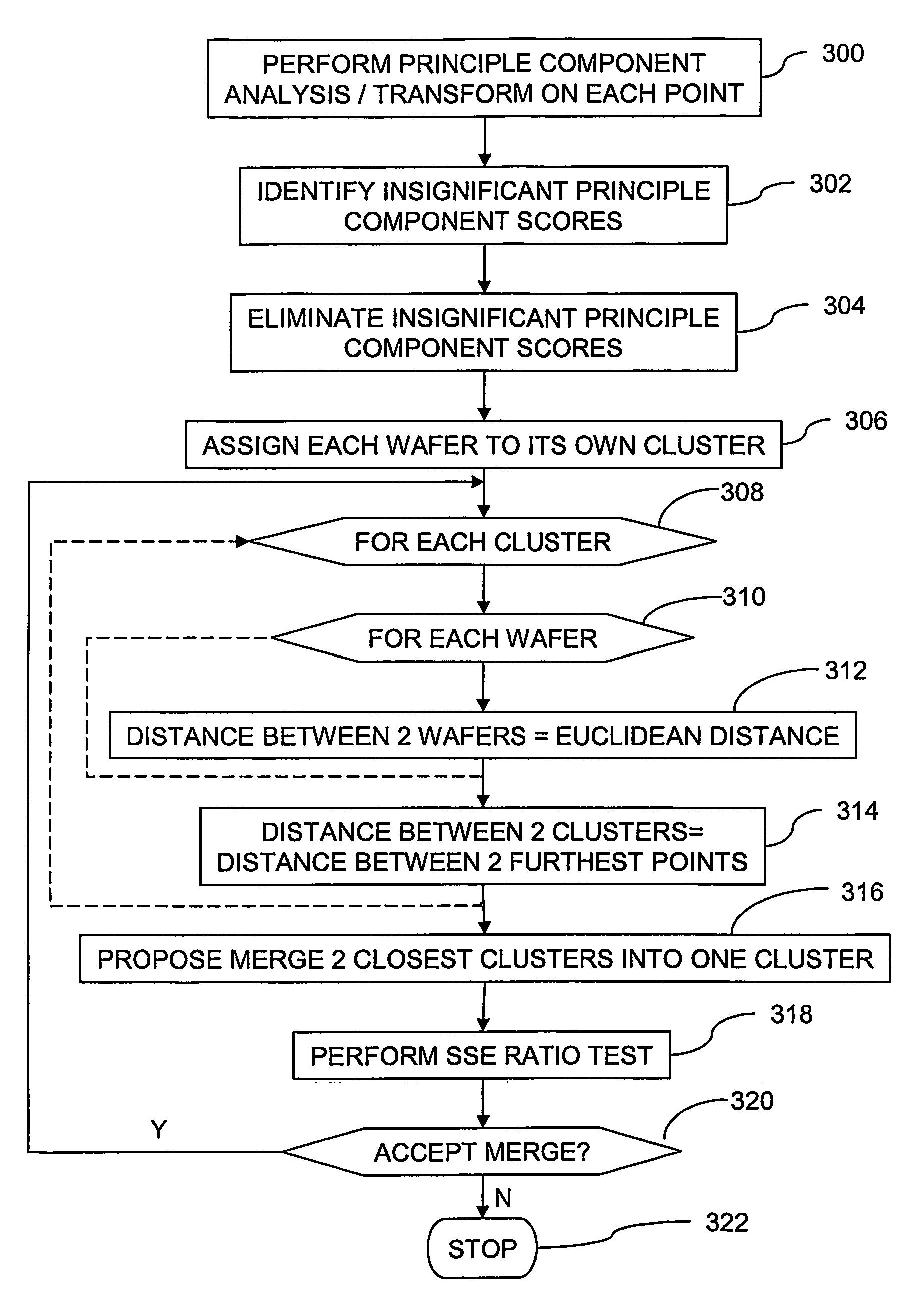
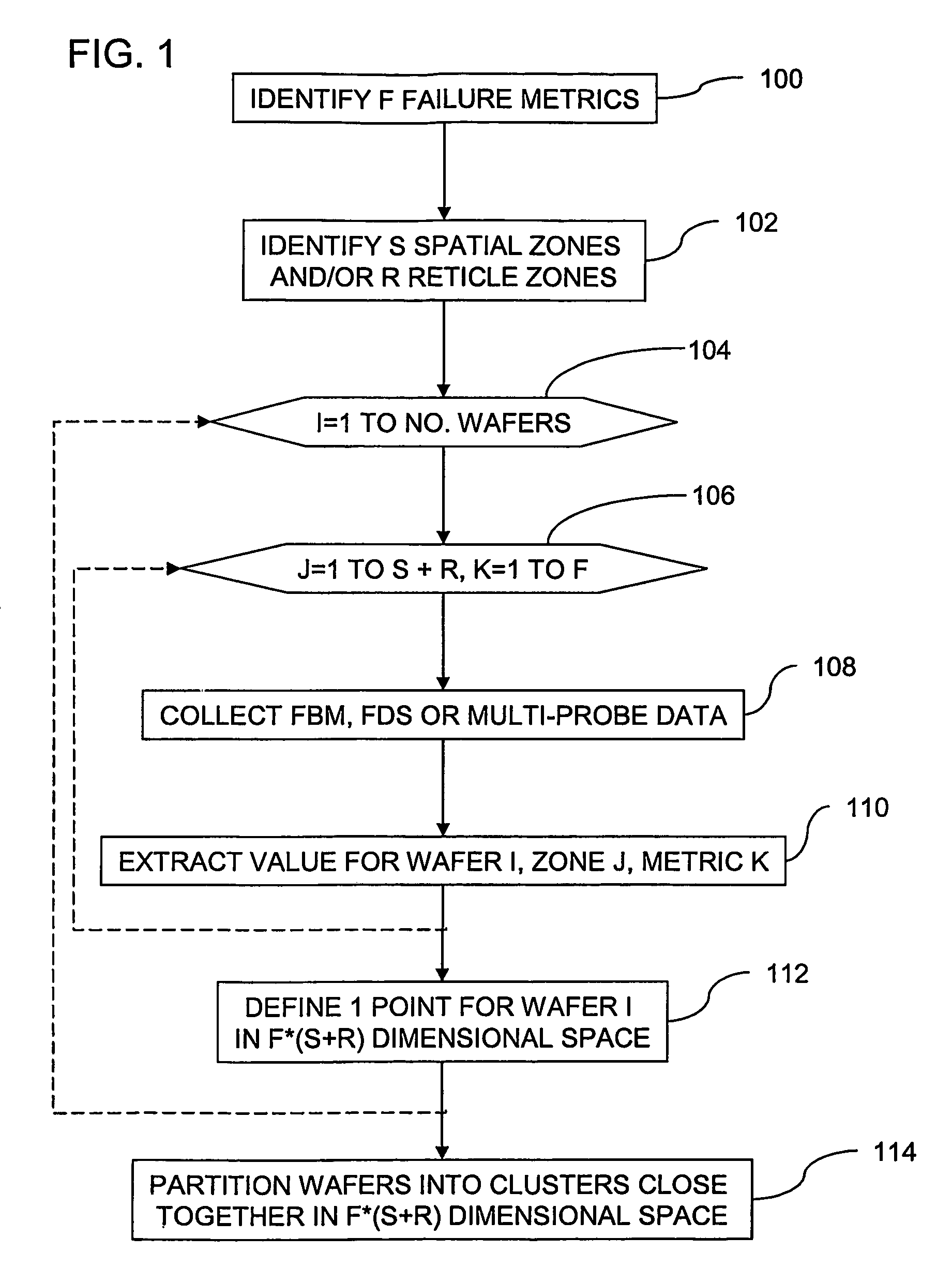
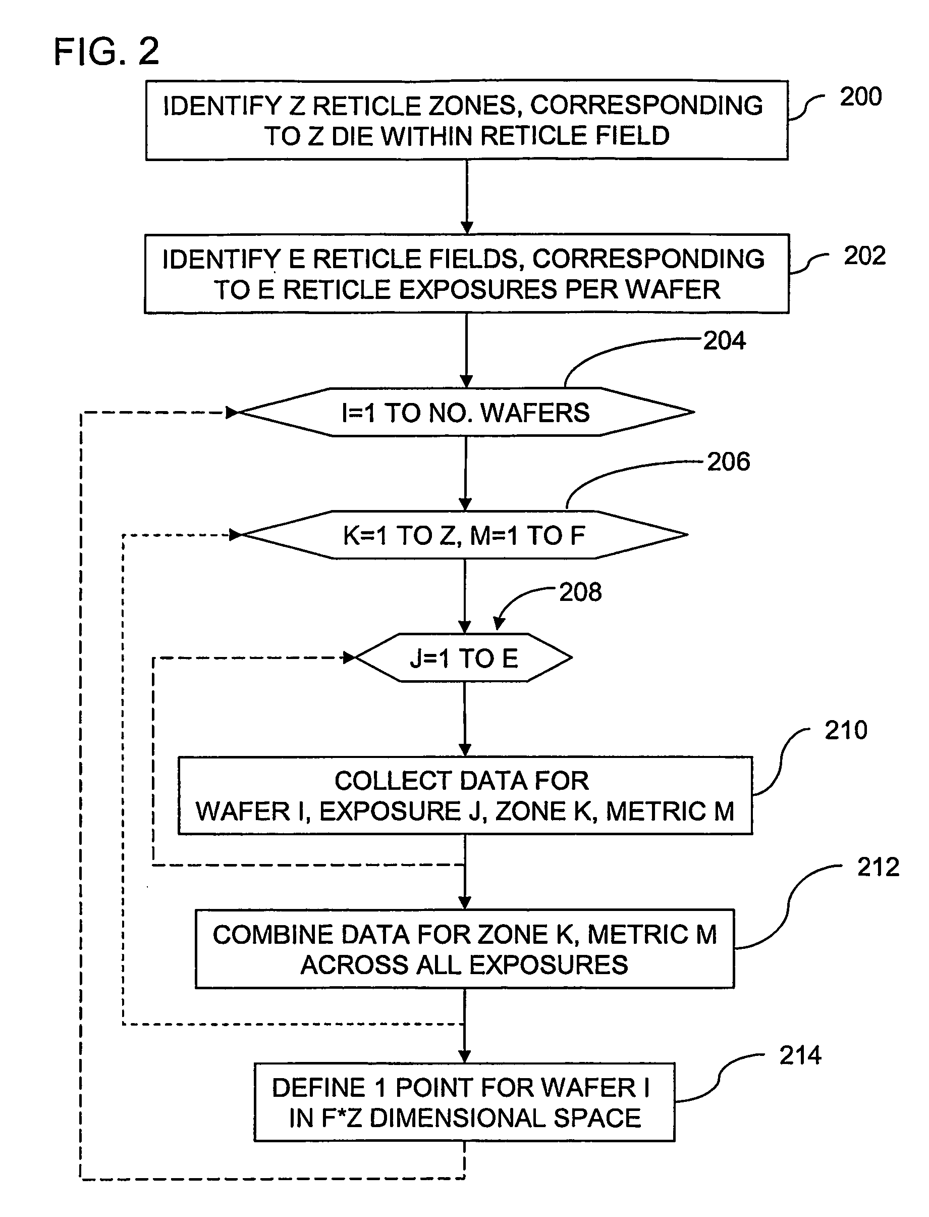
[0025]The methods disclosed herein address the identification of the source of the systematic yield loss as derived from the e-test data, by providing a partitioning method to group wafers with similar systematic yield patterns.

[0026]In general, if one could reduce the noise in the system (response and / or predictor variables) by grouping or clustering wafers with similar root causes together, then such data mining method...


PUM


Abstract

A method for analyzing a sample of wafers includes identifying F failure metrics applicable to at least one pattern on each wafer within the sample. Z spatial and / or reticle zones are identified on each wafer, where Z and F are integers. Values are provided for each failure metric, for each zone on each wafer. A point is defined for each respective wafer in an N-dimensional space, where N=F*Z, and each point has coordinates corresponding to values of the F failure metrics in each of the zones of the corresponding wafer. The sample of wafers is partitioned into a plurality of clusters, so that the wafers within each clusters are close to each other in the N-dimensional space. A plurality of clusters is thus identified from the sample of wafers so that within each individual cluster, the wafers have similar defects to each other.

Description

FIELD OF THE INVENTION[0001]The present invention relates to semiconductor fabrication generally, and more specifically to methods for analyzing semiconductor yield data.BACKGROUND[0002]The fundamental task of yield analysis is to determine the root cause of yield loss so that the consultant, factory engineer and / or designer can take action to mitigate the yield loss mechanism(s). The fundamental challenge is to connect the yield loss, as manifested in failure bit map (FBM) failures or die sort fail bins, as presented by e-test data, to its root cause. Typically, the source of the bin failures from the test data is unknown, but without this information a course of action cannot be taken to resolve the issue. Standard techniques for finding yield loss mechanisms include correlation analysis of yield vs. inline data, e-test data, defect, or wafer process history data. However, straightforward correlation analysis is hampered by the fact that in the manufacture of IC's, hundreds of pro...

Claims


Application Information

Patent Timeline
Patent Type & Authority Patents(United States)
IPC IPC(8): G06F19/00
CPCG05B23/024
Inventor BURCH, RICHARDLIN, PAULGRAVES, SPENCERANTONISSEN, ERIC
Owner PDF SOLUTIONS INC
Why Eureka
Try Eureka