
Low-power transceiver architectures for programmable logic integrated circuit devices

a technology of integrated circuit devices and transceivers, which is applied in the direction of logic circuit coupling/interface arrangements, instruments, pulse techniques, etc., can solve the problems of increasing the power consumption of pld, affecting the performance of the product, and significant issues for some potential users of the product, so as to reduce power consumption, limit the high-end performance, and reduce power consumption

Active Publication Date: 2008-07-22
TAHOE RES LTD
View PDF2 Cites 16 Cited by
  • Summary
  • Abstract
  • Description
  • Claims
  • Application Information

AI Technical Summary

Benefits of technology

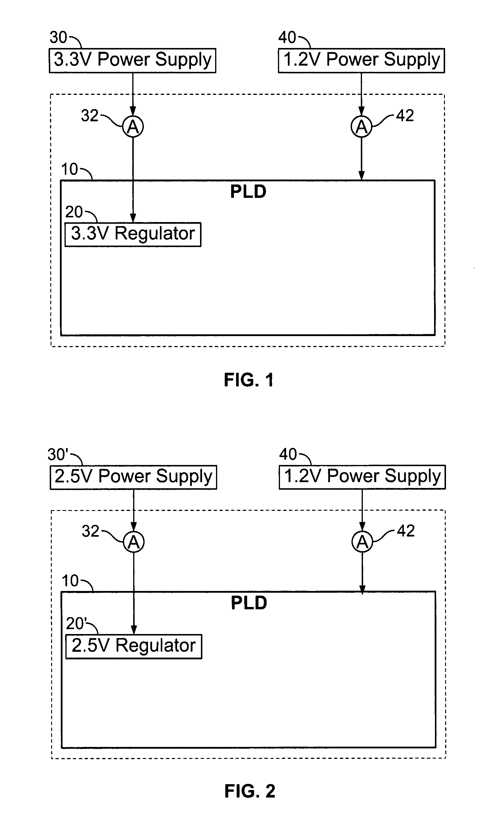
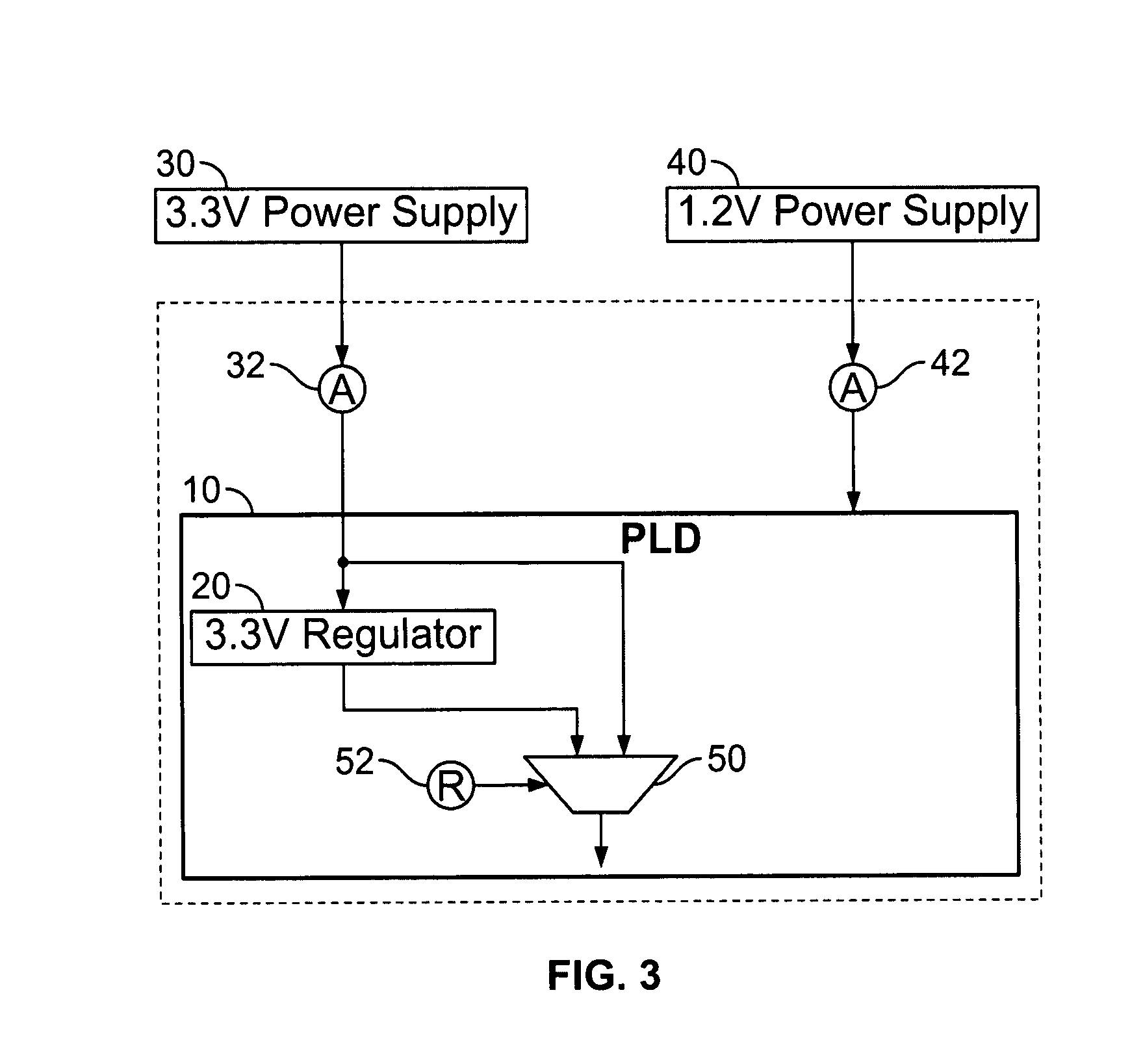
[0004]In accordance with certain possible aspects of the invention, the power consumed by a PLD that includes core circuitry and high-speed serial interface (“HSSI”) or transceiver circuitry can be reduced by reducing the voltage of an external power supply and an internal regulator that collectively supply power to at least some components of the high-speed serial interface circuitry. This may be possible for applications of the PLD for which reduced power consumption is important. It may limit the high-end performance attainable by the PLD, but that may be acceptable in exchange for reduced power consumption.
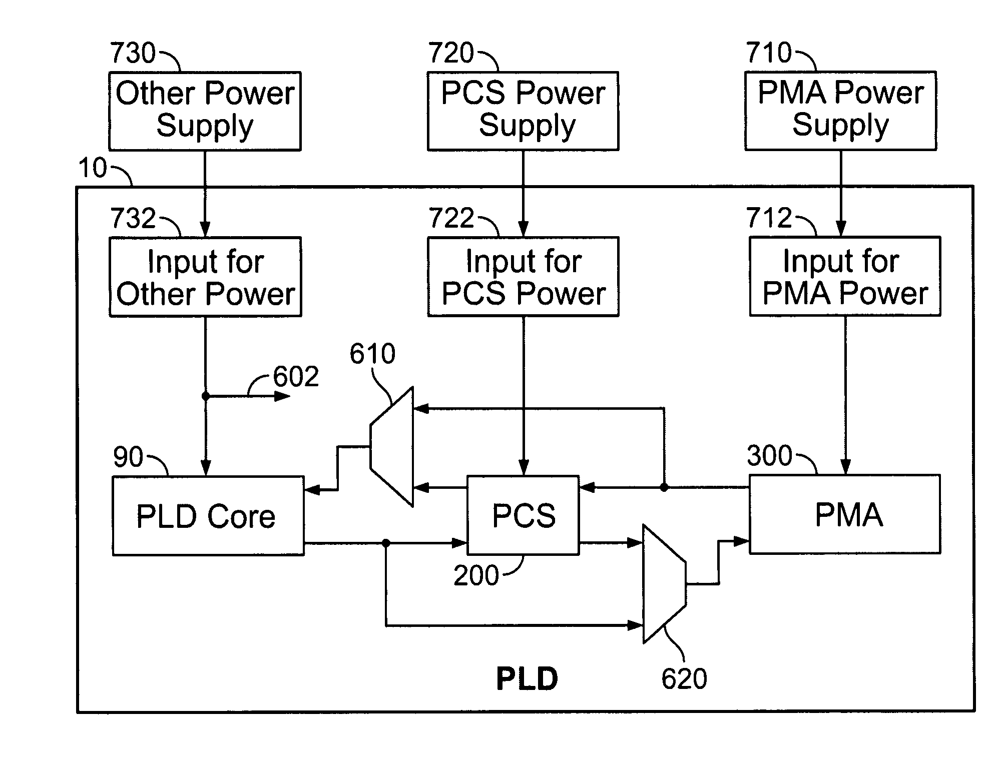
[0007]Other possible aspects of the invention relate to how protocol coding sublayer (“PCS”) circuitry in the HSSI circuitry is used and powered. The protocol coding sublayer is provided for processing signals that are in transit between the PMA and the core (e.g., programmable logic) circuitry of the PLD. The PCS circuitry is primarily digital circuitry (in contrast to the PMA, which typically includes significant analog aspects). In accordance with the present invention, bypass circuitry can be provided for allowing the PCS to be selectively bypassed. If the bypass route is employed, signals travel more directly between the PMA and the core (i.e., without passing through the PCS). Such bypass routing can be used, for example, for applications that involve relatively low data rates. In that event, PCS power can be saved by gating off the clock signal or signals that would otherwise go to the PCS and / or by powering down the PCs.

Problems solved by technology

Giving a PLD product a range of capabilities has a tendency to increase power consumption of the PLD.
This can be a significant issue for some potential users of the product.
Certain aspects of being able to do this may significantly contribute to PLD power consumption.

Method used


Image

  • Low-power transceiver architectures for programmable logic integrated circuit devices
  • Low-power transceiver architectures for programmable logic integrated circuit devices
  • Low-power transceiver architectures for programmable logic integrated circuit devices

Examples


Embodiment Construction

[0021]By way of further brief background, a universal, wide-range transceiver gives convenience to PLD users with respect to such considerations as selecting a system data rate and future system upgrades. However, the performance requirements of higher data rates, as supported by such a transceiver, may constitute a power burden for those users who are only interested in the lower part of the transceiver data range. For some users, power consumption may be a key issue in selecting a PLD vendor. It is therefore desirable to give power consumption an important role in the design of a PLD architecture. In addition, each successive technology node (e.g., each successive major advance in integrated circuit (“IC”) fabrication technology) tends to increase the degree to which transceiver circuit components can be integrated (e.g., placed closer to one another on the PLD). This can bring system noise considerations into architectural decision-making. It is customary to integrate regulators ...


PUM


Abstract

High-speed serial interface or transceiver circuitry on a programmable logic device integrated circuit (“PLD”) includes features that permit the PLD to satisfy a wide range of possible user needs or applications. This range includes both high-performance applications and applications in which reduced power consumption by the PLD is important. In the latter case, any one or more of various features can be used to help reduce power consumption.

Description

BACKGROUND OF THE INVENTION[0001]This invention relates to programmable logic integrated circuit devices (“PLDs”), and more particularly to input / output (transceiver) circuitry for use on PLDs.[0002]PLDs are typically intended to be relatively general-purpose devices. This means that a PLD product is typically designed to be able to support any of a range of uses to which various users may wish to put the device. By enabling one PLD product to satisfy such a range of possible uses, the size of the market for the product can be increased. Increased sales volume can help lower the unit cost of the product.[0003]Giving a PLD product a range of capabilities has a tendency to increase power consumption of the PLD. This can be a significant issue for some potential users of the product. Accordingly, it can be desirable to find ways to give a PLD product a wide range of capabilities and at the same time to reduce power consumption of the PLD, especially when certain of its capabilities are...

Claims


Application Information

Patent Timeline
Patent Type & Authority Patents(United States)
IPC IPC(8): H01L25/00H03K19/177
CPCH03K19/17784H03K19/17744
Inventor SHUMARAYEV, SERGEYWONG, WILSONHOANG, TIM TRITRAN, THUNGOC M.CLIFF, RICHARD G.
Owner TAHOE RES LTD
Learn More