Memory device and method for reading data

a memory device and data technology, applied in the field of memory devices, can solve problems such as programming failure, and achieve the effect of simple circuit for writing

Active Publication Date: 2008-06-24
ALTIS SEMICON +1
View PDF5 Cites 9 Cited by
  • Summary
  • Abstract
  • Description
  • Claims
  • Application Information

AI Technical Summary

Benefits of technology

[0007]The present invention provides a memory device with memory cells comprising resistive elements and a selective switch with an improved controlling of the voltages for reading data from the memory cell. A further embodiment of the present invention provides a memory with voltage levels that improve the reading of data from a memory cell with a resistive element and a selective switch. Furthermore, another embodiment of the present invention provides a memory with memory cells comprising resistive elements and a selective switch, with a first and a second bit line of a bit line pair that are connectable with a first and a second voltage level for attaining an improved memory retention. A further embodiment of the present invention provides an improved method for reading a datum from a memory cell of a memory, wherein the memory cell comprises a resistive element and a switch.
[0011]The present invention provides an improved memory with memory cells comprising resistive elements and a selective switch with a simple circuit for writing and / or reading data from the memory cells. The present invention provides the advantage that conventional circuit arrangements of dynamic random access memory can be used, at least partially, for reading out and / or writing in data in the memory cells. This has the advantage that the input and / or the output of the memory device of the present invention may be modified from a conventional DRAM memory device.

Problems solved by technology

However, voltage cross talk may occur between the high voltage level of a selected bit line, used for programming a selected PMC cell, and a non-selected (or floating) neighbouring bit line that could cause a programming failure.

Method used


Image

  • Memory device and method for reading data
  • Memory device and method for reading data
  • Memory device and method for reading data

Examples


Embodiment Construction

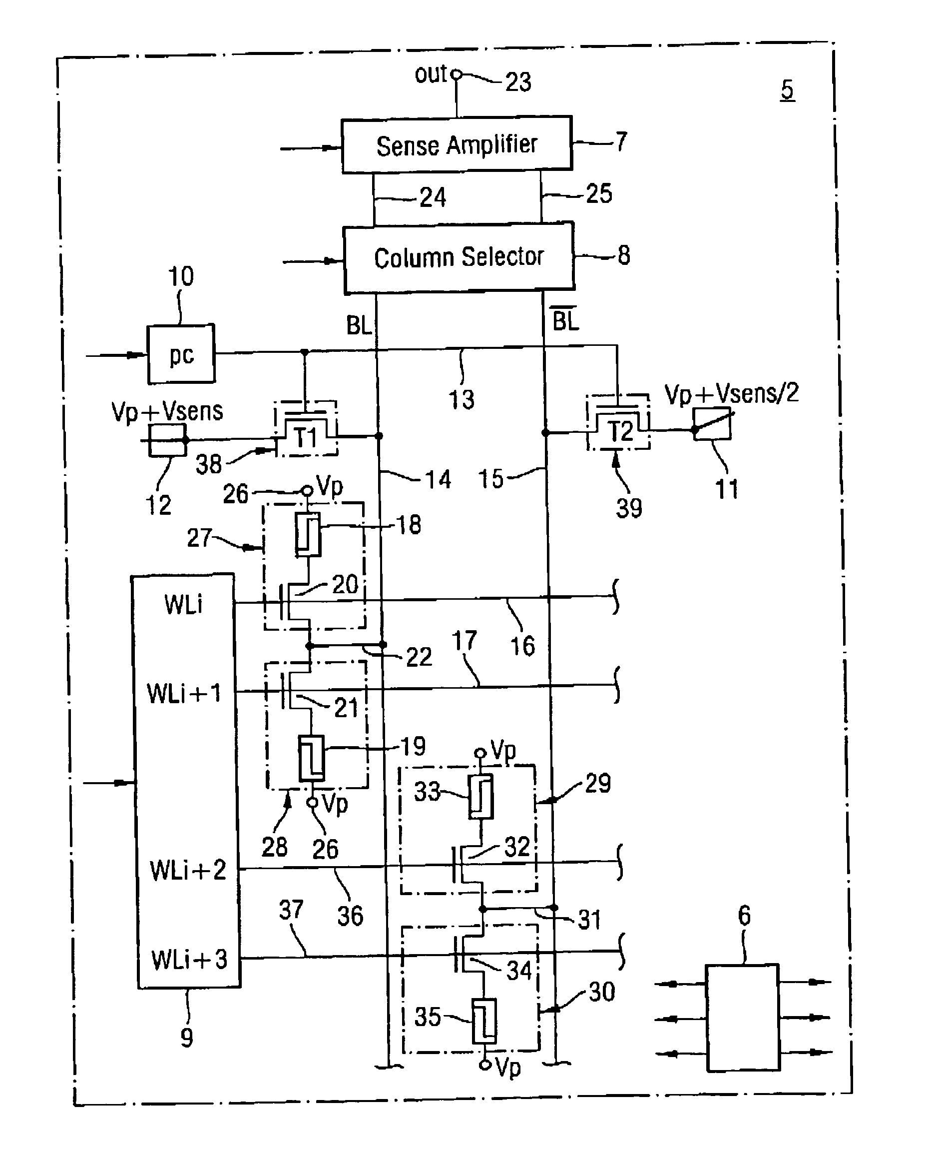
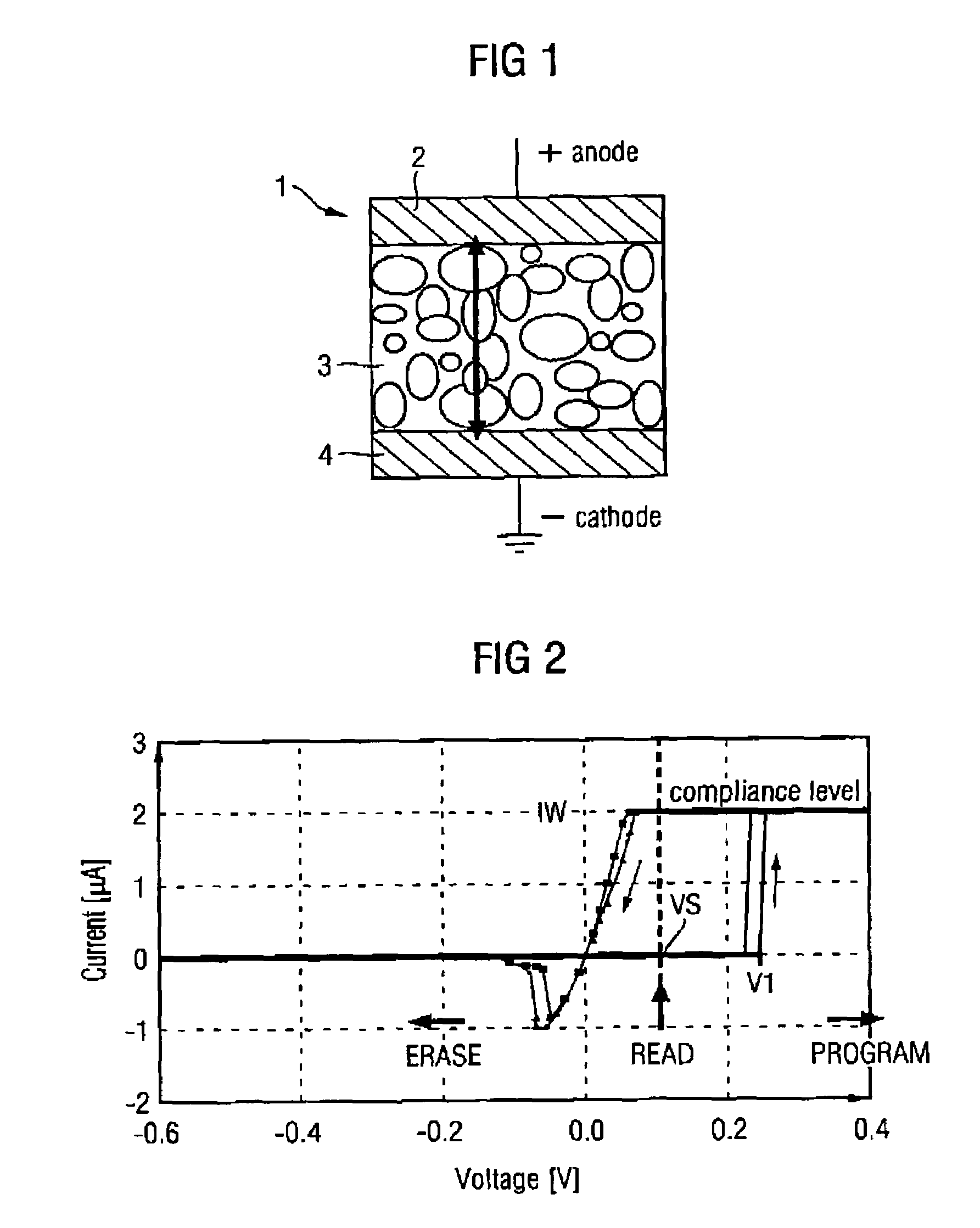
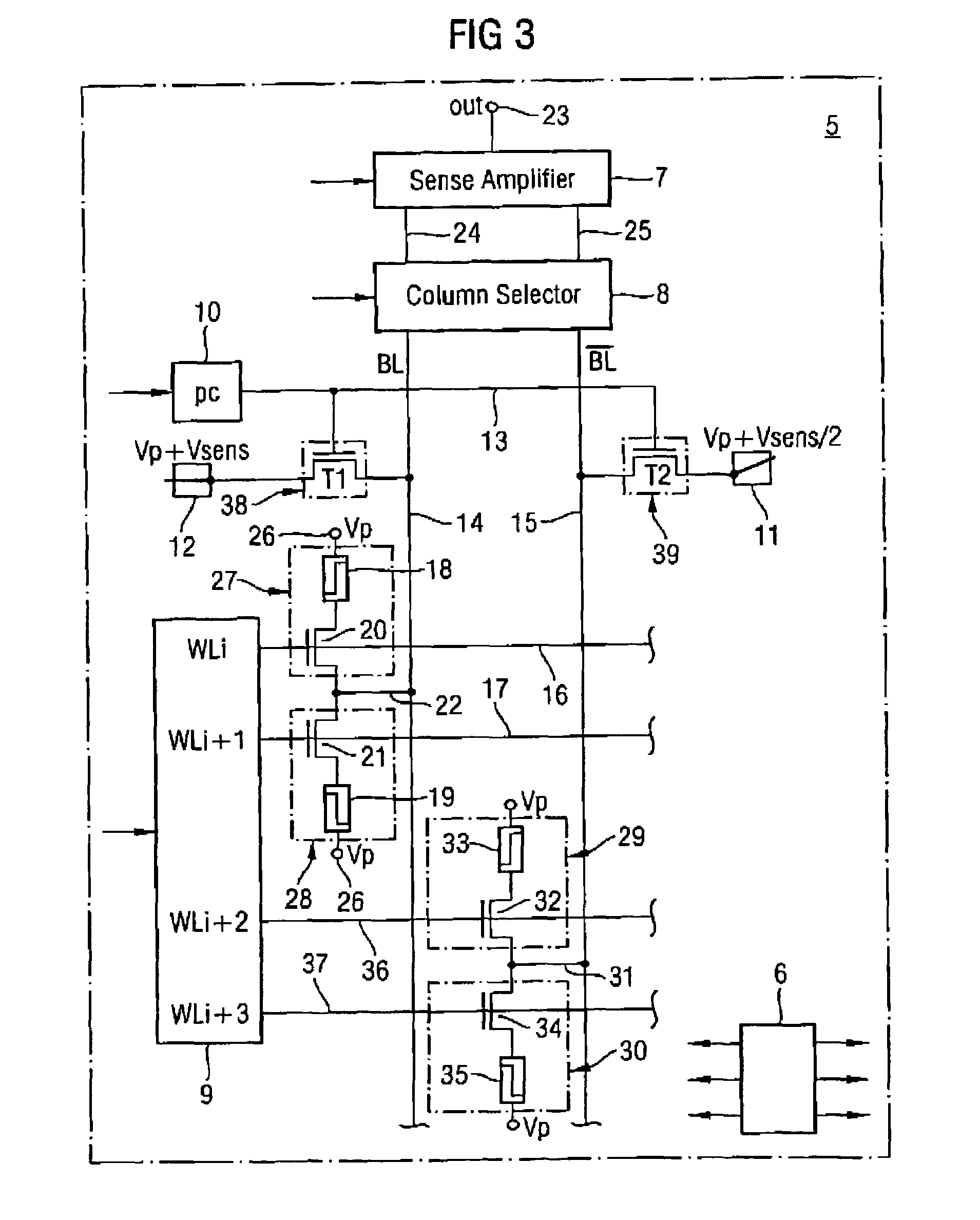
[0019]The present invention generally relates to microelectronic devices. More particularly, the invention relates to programmable structures suitable for various integrated circuit applications, for example, in memory devices.

[0020]The present invention may be described in terms of various functional components. It should be appreciated that such functional components may be realized by any number of hardware or structural components configured to perform the specified functions. For example, the present invention may employ various integrated components comprised of various electrically devices, such as resistors, transistors, capacitors, diodes and such components, the behaviour of which may be suitably configured for various intended purposes. In addition, the present invention may be practised in any integrated circuit application where an effective reversible polarity is desired. Such general applications may be appreciated by those skilled in the art in light of the present d...


PUM


Abstract

A memory with memory cells, wherein a memory cell includes a resistive element and a switch, wherein the memory cells are connected with a common plate line and with respective bit lines, wherein the common plate line supplies a plate voltage, wherein the switches include control inputs that are connected with word lines for controlling the switching states, wherein the word lines are connected with a word line driver that supplies selected word lines with a voltage, wherein the bit lines are connected with second switches, wherein the first bit lines are connectable by respective second switches with a first voltage level and the second bit lines are connectable by respective second switches with a second voltage level, wherein a first and a second bit line are connectable as a bit line pair with a sense amplifier, wherein the sense amplifier amplifies a voltage difference between the first and the second bit line of the bit line pair, wherein the resistive element is able to change the resistance depending on an electrical voltage that is applied across the resistive element, and wherein the second voltage level is between the plate voltage level and the first voltage level.

Description

BACKGROUND OF THE INVENTION[0001]1. Field of the Invention[0002]The invention relates to a memory device with memory cells comprising a resistive element and a selective switch and a method for reading a datum from a memory cell of a memory device comprising a resistive element.[0003]2. Description of the Related Art[0004]Memory cells with resistive elements and a selective switch, having for example, a solid electrolyte material as a resistive material, are well known as programmable metallization cells (PMC). Memory device including such PMC memory cells are known as conductive-bridging random access memory (CBRAM). The storing of different states in a PMC memory cell is based on the developing or diminishing of a conductive path in the electrolyte material between electrodes based on an applied electric field. Since the electrolyte material has a high resistance and the conductive path between electrodes has a low resistance, the PMC memory cell can be set to different states dep...

Claims


Application Information

Patent Timeline
Patent Type & Authority Patents(United States)
IPC IPC(8): G11C11/00
CPCG11C7/12G11C13/0011G11C13/0026G11C13/004G11C13/04G11C2013/0042G11C2213/79
Inventor GOGL, DIETMAR
Owner ALTIS SEMICON
Why Eureka
Try Eureka