
Chip blanking and processing in SCDMA to mitigate impulse and burst noise and/or distortion

a technology of scdma and chip blanking, applied in the field of information transfer, to achieve the effect of reducing impairmen

Inactive Publication Date: 2008-04-29
AVAGO TECH INT SALES PTE LTD
View PDF6 Cites 18 Cited by
  • Summary
  • Abstract
  • Description
  • Claims
  • Application Information

AI Technical Summary

Benefits of technology

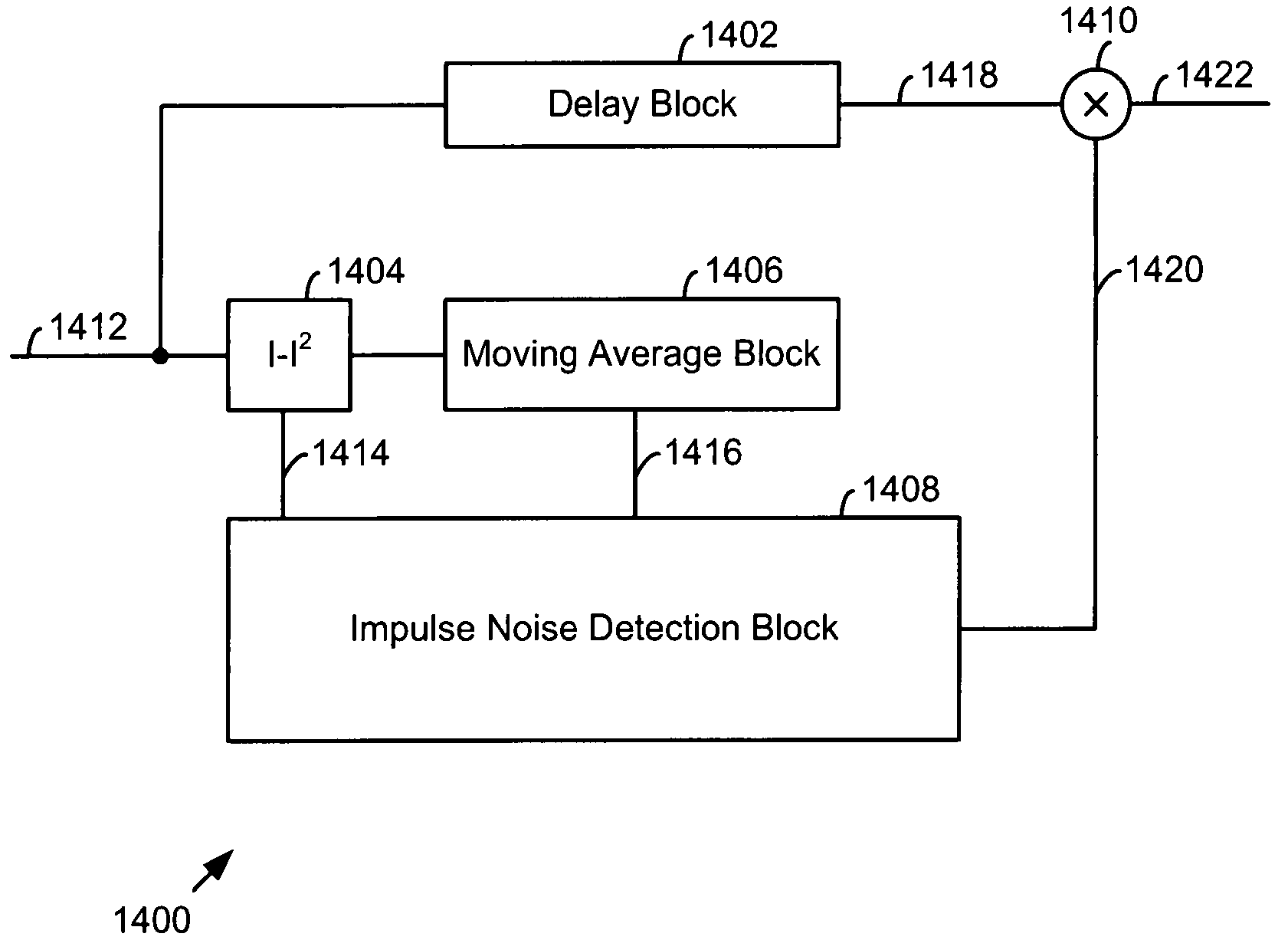
The present invention is a system for improving communication by mitigating impairment. The system includes a delay block, a signal level block, a moving average window block, an impulse noise detection block, and a combiner. The delay block receives and delays each chip in a spreading interval, which may have a duration of 128 chips in an SCDMA system. The signal level block determines the signal level of each chip in the spreading interval. The moving average window block combines the signal level of each chip in a chip window to determine the composite signal level of the chip window. The impulse noise detection block receives the signal level and the composite signal level and produces an erasure indication for each chip. The combiner then erases the chips based on the erasure indication. The erased and kept chips are then passed to a despreader that despreads the chips across the spreading interval to produce a symbol for the spreading interval. The invention helps to improve communication quality by detecting and eliminating impairments caused by impulse noise.

Problems solved by technology

Further, the system may operate across different spreading sequences whose boundaries are affected by an impairment.

Method used


Image

  • Chip blanking and processing in SCDMA to mitigate impulse and burst noise and/or distortion
  • Chip blanking and processing in SCDMA to mitigate impulse and burst noise and/or distortion
  • Chip blanking and processing in SCDMA to mitigate impulse and burst noise and/or distortion

Examples


first embodiment

[0118]FIG. 16 is a flow diagram illustrating operation according to the present invention for mitigating impairment in a communication system. As shown in FIG. 16, operation commences in receiving a plurality of chips in a spreading interval (step 1602). Each chip is considered separately in the operation of FIG. 16. As a first operation for each chip in the spreading interval, the signal level of the chip is determined (step 1604). As was previously described, this chip level is determined in one embodiment by magnitude-squaring a measured level of the chip. Because most chips have complex components, and are spread by either a 1 or −1 chip such summation is required so that a valid comparison between the signal level and a threshold and between the signal levels of adjacent chips can be made.

[0119]Operation continues in comparing the signal level of the chip to a first threshold to produce a first comparison result (step 1606). Then, operation continues by determining the composit...

second embodiment

[0123]FIG. 17 is a flow diagram illustrating operation according to the present invention for mitigating impairment in a communication system. The operations of steps 1702 through 1710 correspond to operations of steps 1602 through 1610 of FIG. 16 and are not separately described with reference to FIG. 17. However, additional operations in FIG. 17 include comparing the composite signal level of the plurality of chips of the corresponding chip window to a third threshold to produce a third comparison result (step 1712). Operations further include determining a fourth comparison result based upon the third comparison result of adjacent chips (step 1714). Then, the decision whether to keep or erase the chip is further based upon the fourth comparison result. Thus, the operation at step 1716 includes determining the erasure indication based upon the first comparison result, the second comparison result, and the fourth comparison result. The fourth comparison is based upon the third comp...


PUM


Abstract

A system for mitigating impairment in a communication system includes a delay block, a signal level block, a moving average window block, an impulse noise detection block, and a combiner. The delay block receives and delays each chip of a plurality of chips in a spreading interval. The signal level block determines a signal level of each chip of the plurality of chips in the spreading interval. The moving average window block determines a composite signal level for a chip window corresponding to the chip. The impulse noise detection block receives the signal level, receives the composite signal level, and produces an erasure indication for each chip of the plurality of chips of the corresponding chip window. The combiner erases chips of the plurality of chips of the spreading interval based upon the erasure indication.

Description

CROSS-REFERENCE TO RELATED APPLICATIONS[0001]This application is a continuation-in-part of application Ser. No. 10 / 136,059 filed Apr. 30, 2002, which became an U.S. Pat. No. 7,236,545, which claims benefit of and priority from, Provisional Application No. 60 / 296,884 filed Jun. 8, 2001, titled “Detection and Mitigation of Temporary Impairments in a Communications Channel”, the complete subject matter of each of which is incorporated herein by reference in its entirety.FEDERALLY SPONSORED RESEARCH OR DEVELOPMENT[0002][Not Applicable]SEQUENCE LISTING[0003][Not Applicable]MICROFICHE / COPYRIGHT REFERENCE[0004][Not Applicable]BACKGROUND OF THE INVENTION[0005]The present invention relates to communications systems, all of which are inherently limited in their capacity (or rate) of information transfer by channel impairments. More specifically, the present invention relates to information transfer between a plurality of Cable Modems (alternatively referred to as “CM”) and a Cable Termination...

Claims


Application Information

Patent Timeline
Patent Type & Authority Patents(United States)
IPC IPC(8): H04L27/06H04B1/707H04J3/06H04L1/00
CPCH04B1/71H04B1/7103H04B1/71072H04L1/0003H04L1/0009H04L1/0045H04L1/005H04L1/0057H04N21/6168H04B1/7102H04B1/71055H04B2201/709709
Inventor KOLZE, THOMAS J.YOUSEF, NABIL R.MIN, JONATHAN S.
Owner AVAGO TECH INT SALES PTE LTD
Learn More