
Compressed encoding for repair

a technology of compressed encoding and repair, which is applied in the field of repair of embedded memory devices, can solve the problems of increasing the complexity of the circuitry formed on the chip, increasing the complexity of the testing required to ensure the circuitry functions correctly, and making conventional testing using external test equipment extremely difficul

Active Publication Date: 2008-03-25
ADVANCED MICRO DEVICES INC
View PDF9 Cites 82 Cited by
  • Summary
  • Abstract
  • Description
  • Claims
  • Application Information

AI Technical Summary

Benefits of technology

The patent describes a method and mechanism for repairing devices using a built-in self-repair (BISR) mechanism. The repair information is stored in a compressed format and can be easily identified. The encoding of repairs includes a format that identifies different parts of the device and their corresponding levels of hierarchy. The repair encoding includes bits that indicate which parts of the device are targeted by the repair. The technical effect of this patent is to provide a more efficient and effective way to repair devices by identifying and targeting specific parts of the device that require attention.

Problems solved by technology

As the complexity of circuitry formed upon chips increases, the complexity of the testing required to ensure the circuitry functions correctly also increases.
However, conventional testing using external test equipment is made extremely difficult as much of the circuitry formed on integrated circuit chips is typically not controllable or observable from input / output (I / O) pads.
In addition to the above, increasing size, density and complexity in memory technologies lead to higher defect density and a corresponding decrease in yield.
However, directly associating fuses with repair elements on a CPU die with many arrays may be inefficient as it is likely that only a few repairs may need to be done.
If many repairs need to be done to the arrays, it is likely that there would be a defect in the logic as well and the die may be unsalvageable in any event.

Method used


Image

  • Compressed encoding for repair
  • Compressed encoding for repair
  • Compressed encoding for repair

Examples


Embodiment Construction

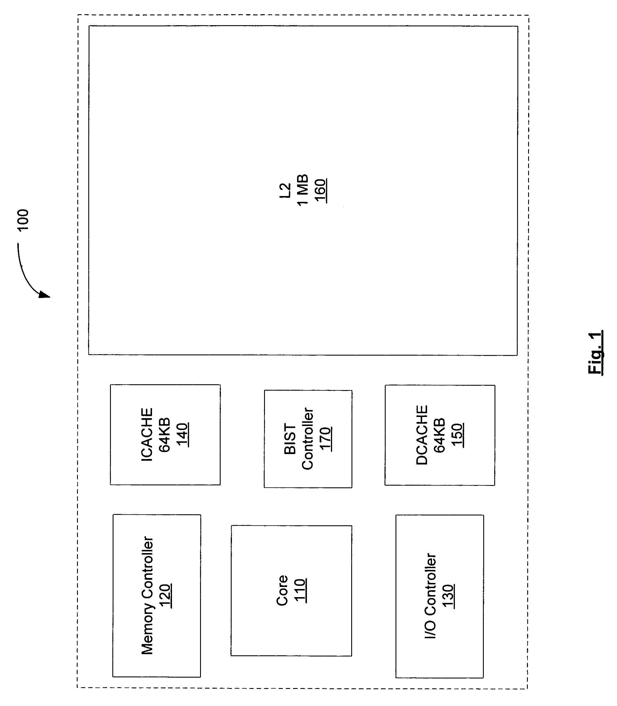
[0022]FIG. 1 illustrates a block diagram of one embodiment of a microprocessor 100 configured to perform self test and repair. In one embodiment, each of the components illustrated in FIG. 1 may be manufactured on a single die. Processor 100 includes a core 110, memory controller 120, I / O controller 130, instruction cache (Icache) 140, data cache (Dcache) 150, level 2 (L2) cache 160 and built in self test (BIST) controller 170. Icache 140 and Dcache 150 may be level 1 (L1) caches. For purposes of discussion, assume the L2 cache includes 1 MByte of storage, while each of the instruction 140 and data 150 caches includes 64 Kbytes of storage. Consequently, the L2 cache 160 is configured to store 16 times the data of either the Icache 140 or the Dcache 150. The cache blocks in the block diagram have been drawn to approximate the relative size of each of the caches.

[0023]Generally speaking, the likelihood of a defect in a component of a die corresponds to the amount of area occupied by t...


PUM


Abstract

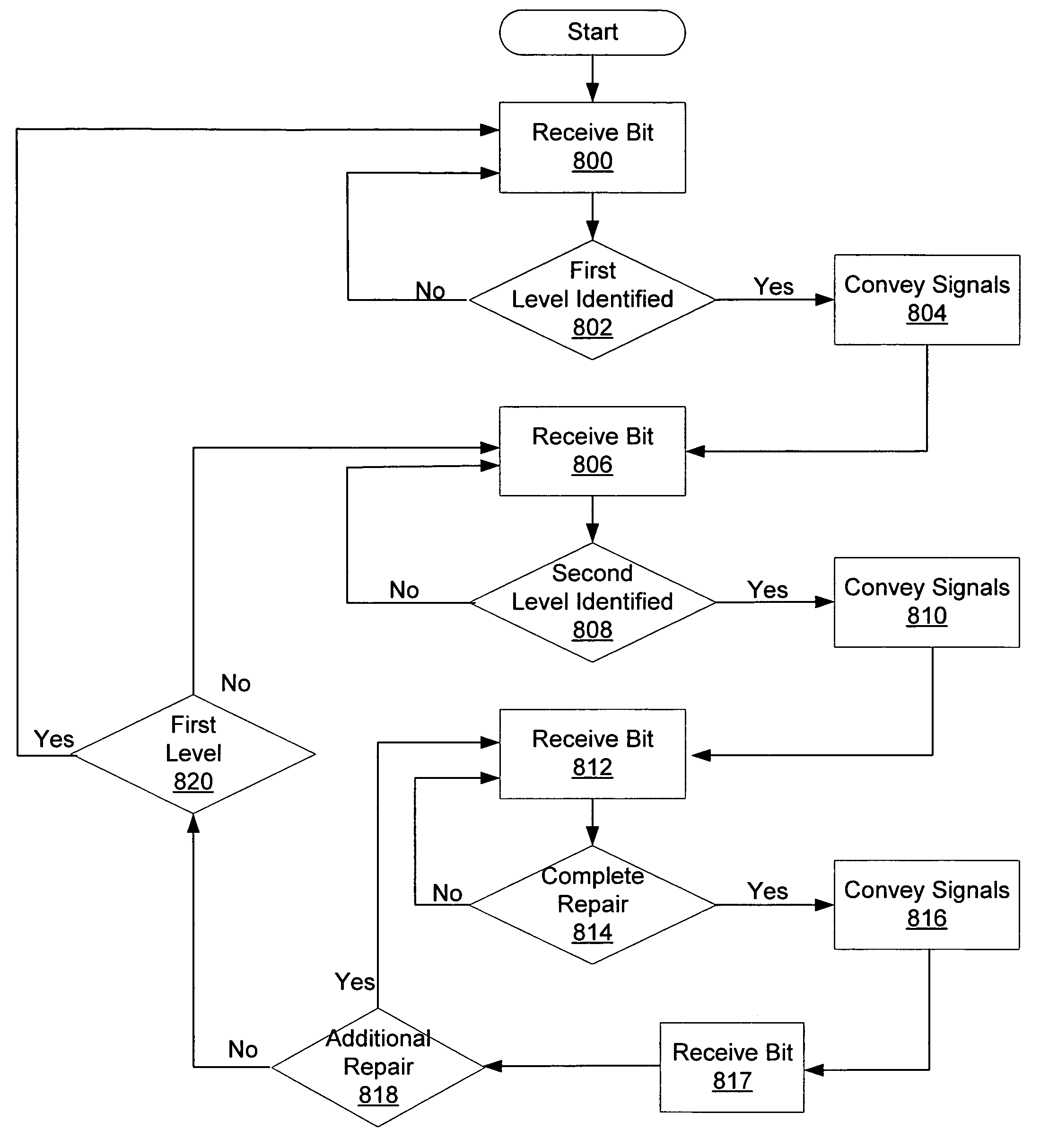
A hierarchical encoding format for coding repairs to devices within a computing system. A device, such as a cache memory, is logically partitioned into a plurality of sub-portions. Various portions of the sub-portions are identifiable as different levels of hierarchy of the device. A first sub-portion may corresponds to a particular cache, a second sub-portion may correspond to a particular way of the cache, and so on. The encoding format comprises a series of bits with a first portion corresponding to a first level of the hierarchy, and a second portion of the bits corresponds to a second level of the hierarchy. Each of the first and second portions of bits are preceded by a different valued bit which serves to identify the hierarchy to which the following bits correspond. A sequence of repairs are encoded as string of bits. The bit which follows a complete repair encoding indicates whether a repair to the currently identified cache is indicated or whether a new cache is targeted by the following repair. Therefore, certain repairs may be encoded without respecifying the entire hierarchy.

Description

BACKGROUND OF THE INVENTION[0001]1. Field of the Invention[0002]This invention relates to integrated circuit testing and repair, and more particularly to the repair of embedded memory devices.[0003]2. Description of the Related Art[0004]Advances in integrated circuit fabrication technology continue to enhance the ability to form increasingly more circuitry upon integrated circuit chips. As the complexity of circuitry formed upon chips increases, the complexity of the testing required to ensure the circuitry functions correctly also increases. However, conventional testing using external test equipment is made extremely difficult as much of the circuitry formed on integrated circuit chips is typically not controllable or observable from input / output (I / O) pads. This is especially true of memory arrays formed along with random logic circuitry upon integrated circuit chips (i.e., embedded memory arrays). A solution to the chip testing problem increasingly being adopted is to incorporat...

Claims


Application Information

Patent Timeline
Patent Type & Authority Patents(United States)
IPC IPC(8): G11C29/00G11C7/00
CPCG06F12/0802G11C29/44G11C29/4401G11C29/802G11C2029/0401
Inventor ZURASKI, JR., GERALD D.WHITE, SCOTT A.
Owner ADVANCED MICRO DEVICES INC
Learn More