
Wafer container door with particulate collecting structure

a technology of particulate collection and container door, which is applied in the direction of transportation and packaging, other domestic articles, packaging goods types, etc., can solve the problems of high cost, easy damage by physical and electrical shock, and high cost of semiconductor wafers, and achieves the effects of reducing the risk of contamination, and reducing the service life of the container door

Inactive Publication Date: 2008-02-05
ENTEGRIS INC
View PDF10 Cites 11 Cited by
  • Summary
  • Abstract
  • Description
  • Claims
  • Application Information

AI Technical Summary

Benefits of technology

"The present invention provides a wafer container with a particle capture feature that collects and captures particles or particulates, which helps to prevent them from causing negative visual effects and contamination. The container includes a latch mechanism and a panel with a particle capture region that can be detachably coupled to the chassis, allowing for easy removal of captured particles. The isolated textured region prevents particles from circulating within the door and potentially coming into contact with the wafers, while also reducing the accumulation of particulate matter on the transparent surface."

Problems solved by technology

The wafers are very valuable, extremely delicate, and easily damaged by physical and electrical shocks.
Although wafer enclosures are used in clean environments, undesirable contaminants can accumulate on and in the enclosure over time.
Semiconductor wafer fabrication processes are often extremely sensitive to any contamination.
Over time, the particulate formation can result in visible smudging, smearing, and / or clouding of the transparent plastic door panels.
While this presents an undesirable aesthetic result, such contaminants and particles or particulates also present the risk of entering the enclosure and contaminating the wafers.

Method used


Image

  • Wafer container door with particulate collecting structure
  • Wafer container door with particulate collecting structure
  • Wafer container door with particulate collecting structure

Examples


Embodiment Construction

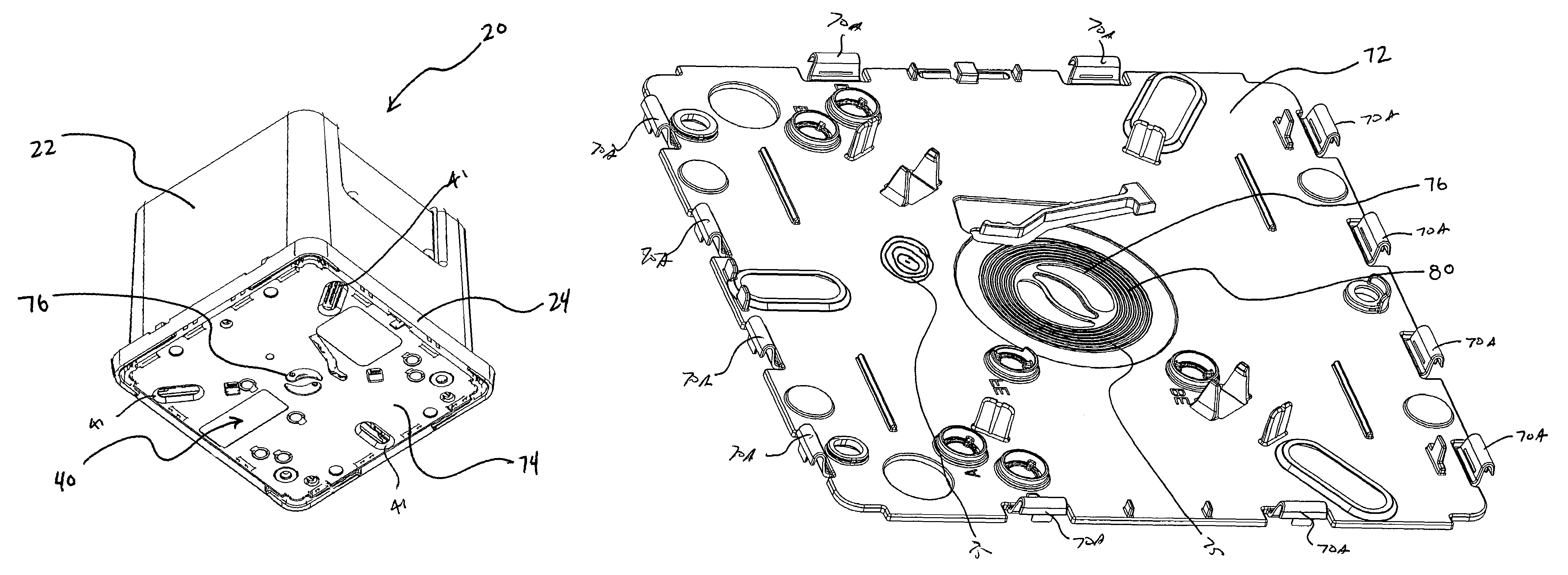
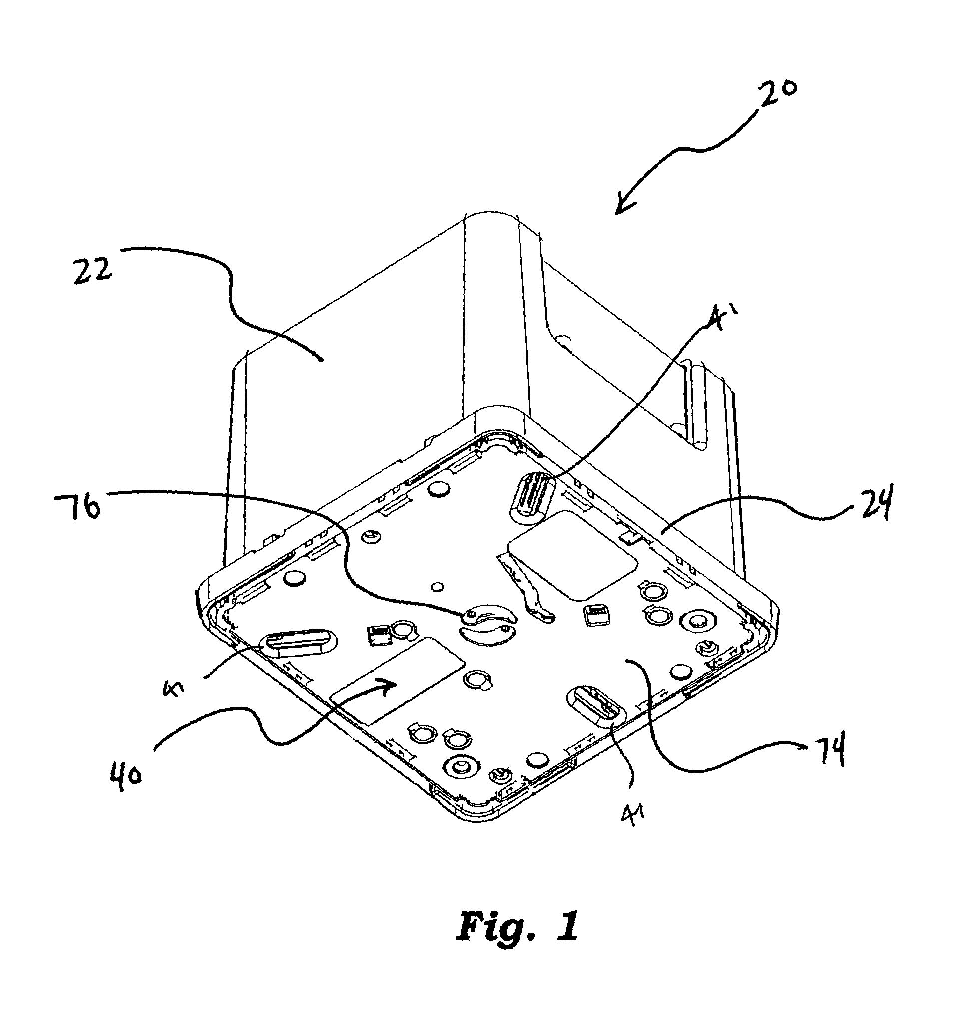
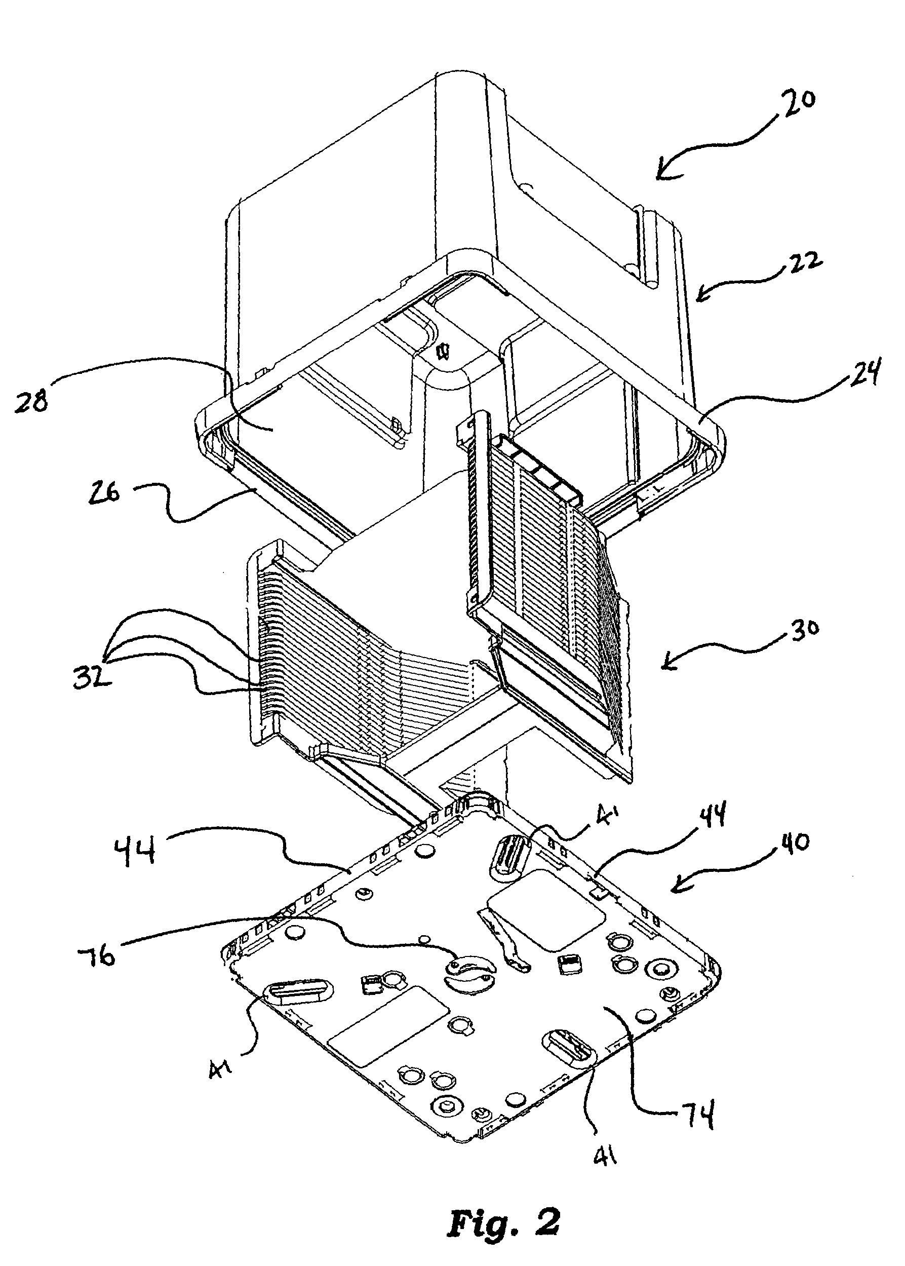
[0025]A substrate container 20 for carrying substrates is depicted in FIGS. 1-3. Referring to FIG. 2, wafer container 20 generally includes an enclosure 22 having a door frame 24 defining access opening 26 for accessing interior 28 of container 20, cassette 30 having a plurality of slots 32 for receiving and holding wafers (not depicted), and door 40 for sealably closing access opening 26. Door 40 generally includes door chassis portion 40A and panel portion 40B. Door 40 may include a plurality of kinematic coupling grooves 41 for locating and securing container 20 on a piece of processing equipment (not depicted). Door 40 may also include locating structures 41A for receiving and retaining cassette 30. Referring to FIG. 3, door 40 may include top wall 42 and peripheral wall 44 extending away from top wall 42. Peripheral wall 44 and top wall 42 define interior space 46 of door 40. Door 40 may include a gasket 47 along door periphery 47A for sealingly engaging enclosure portion 22. D...


PUM


Abstract

A substrate container having an enclosure with an access opening for inserting and removing substrates into an interior of the enclosure and a door chassis that is configured to selectively enclose the opening, the door chassis comprising a first wall having a peripheral wall extending therefrom. The substrate container includes a latch mechanism that is operably coupled with the chassis, the latch mechanism configured to operably secure the chassis to the opening. The door of the substrate container includes a textured particle capture region wherein particles generated by the latch mechanism and elsewhere are captured by the particle capture region.

Description

[0001]This application claims priority to U.S. Provisional Application 60 / 563,526, filed Apr. 18, 2004, entitled “WAFER CONTAINER DOOR WITH PARTICULATE COLLECTING STRUCTURE,” which is incorporated herein by reference.FIELD OF THE INVENTION[0002]The present invention relates to substrate containers. More particularly, the present invention relates to substrate container doors having textured regions to trap and prevent the circulation of particles or particulates that are generated within the containers.BACKGROUND OF THE INVENTION[0003]Substrate containers are used in the semiconductor processing industry for storing and transporting semiconductor wafers, flat panel substrates, and film frames. Examples of containers that are used in the semiconductor processing industry are FOUPs (front opening unified pods), FOSBs (front opening shipping box), and SMIF (standardized mechanical interface) pods. Such containers generally have an enclosure with an open bottom or side that is sealingly...

Claims


Application Information

Patent Timeline
Patent Type & Authority Patents(United States)
IPC IPC(8): B65D45/16B65D51/24B65D85/86B65D25/54B65D85/30B65D85/00H01L21/673
CPCH01L21/67373H01L21/67393Y10S206/832B65D85/00B65D85/38H01L21/67H01L21/673
Inventor HALBMAIER, DAVID L.
Owner ENTEGRIS INC
Learn More