Calibration standard for transmission electron microscopy

a technology of transmission electron microscope and calibration standard, which is applied in the direction of optical radiation measurement, instruments, semiconductor/solid-state device testing/measurement, etc., can solve the problems of undesirable time delay, high cost, and high labor intensity of calibration personnel, and achieves the effect of reducing labor intensity and reducing labor intensity

Inactive Publication Date: 2007-11-06
BELL SEMICON LLC
View PDF13 Cites 14 Cited by
  • Summary
  • Abstract
  • Description
  • Claims
  • Application Information

AI Technical Summary

Problems solved by technology

Calibration procedures are very time consuming and have a negative impact on semiconductor fabrication workflow.
Typical S/TEM magnification calibration approaches are also limited in accuracy.
Such a standard is only useful over a certain portion of the usable magnification range of an S/TEM, thereby again requiring several different standards having approp...

Method used


Image

  • Calibration standard for transmission electron microscopy
  • Calibration standard for transmission electron microscopy
  • Calibration standard for transmission electron microscopy

Examples


Embodiment Construction

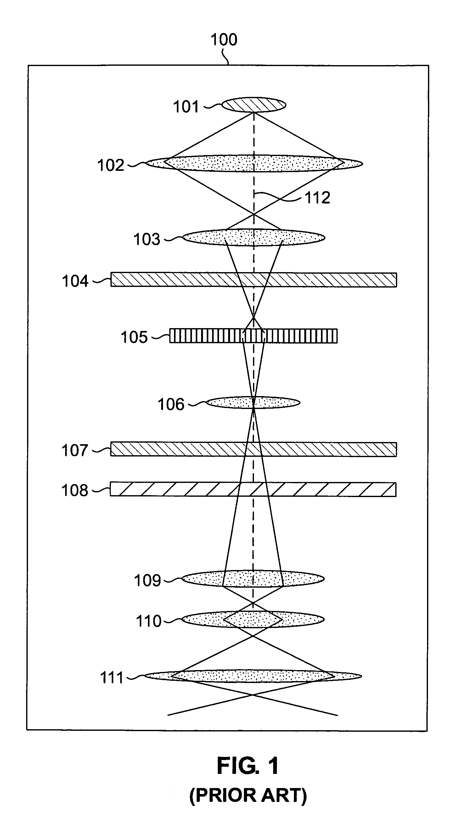
[0011]During fabrication, semiconductor products are analyzed using high-resolution electron microscopy such as Scanning Transmission Electron Microscopes (STEM) and Transmission Electron Microscopes (TEM), sometimes referred to collectively as S / TEM system. A block diagram representing a S / TEM system 100 is provided in FIG. 1 where the energy source represents an electron gun 101 that produces a stream of monochromatic electrons. This stream is focused into a small, thin, coherent beam by the use of condenser lenses 102, 103. The first lens 102 largely determines the “spot size”; the general size range of the final spot that strikes a sample 105. A “spot size knob” usually controls this condenser lens. The second condenser lens 103 changes the spot size on a sample also known as a specimen 105, adjusting the beam from a dispersed spot to a pinpoint beam. An “intensity or brightness knob” controls this lens. The user selected condenser aperture 104 constricts the resulting beam. Thi...


PUM


Abstract

A calibration standard includes a silicon substrate having a plurality of defined regions and a plurality of calibration marks placed on respective defined regions of the silicon substrate. Each calibration mark comprises a different calibration dimension indicator and a corresponding dimension identifier. A method for calibrating a transmission electron microscope using the standard comprises positioning the calibration standard in a viewing area of the transmission electron microscope and sequentially viewing the marks and adjusting the calibration of the microscope for each mark viewed.

Description

FIELD OF THE INVENTION[0001]This invention relates in general to the field of instrument calibration. More particularly, this invention relates to a calibration standard for Transmission Electron Microscopes (TEM).BACKGROUND OF THE INVENTION[0002]Semiconductor manufacturing consists of a number of crucial processing steps performed on wafer lots where measurements of minimum feature sizes known as critical dimensions (CD) are made to ensure proper device fabrication. The high-degree of precision during this processing requires the utilization of Scanning Transmission Electron Microscopes and Transmission Electron Microscopes (S / TEM) to calibrate in line CD-SEM instruments. These critical tools provide measurement capabilities in the low nanometer range. Accuracy of their measurements is essential since effective process controls depend on CDs they supply. S / TEMs require frequent calibration to ensure their accuracy since processing errors cause appreciable variation in CDs. Calibrat...

Claims


Application Information

Patent Timeline
IPC IPC(8): G12B13/00H01L21/66
CPCH01J37/263H01J2237/2826
Inventor BAIOCCHI, FRANK A.DELUCCA, JOHN MICHAELCARGO, JAMES THOMAS
Owner BELL SEMICON LLC
Why Eureka
Try Eureka