Bit line sense amplifier and semiconductor memory device having the same
a technology of bit line sense amplifier and semiconductor memory device, which is applied in the direction of information storage, static storage, digital storage, etc., can solve the problems of difficult to accurately measure the cell capacitance, the offset voltage of the bit line sense amplifier cannot be accurately measured, and the sense amplifier cannot stably perform an amplifying operation
- Summary
- Abstract
- Description
- Claims
- Application Information
AI Technical Summary
Benefits of technology
Problems solved by technology
Method used
Image


Examples
embodiment 1
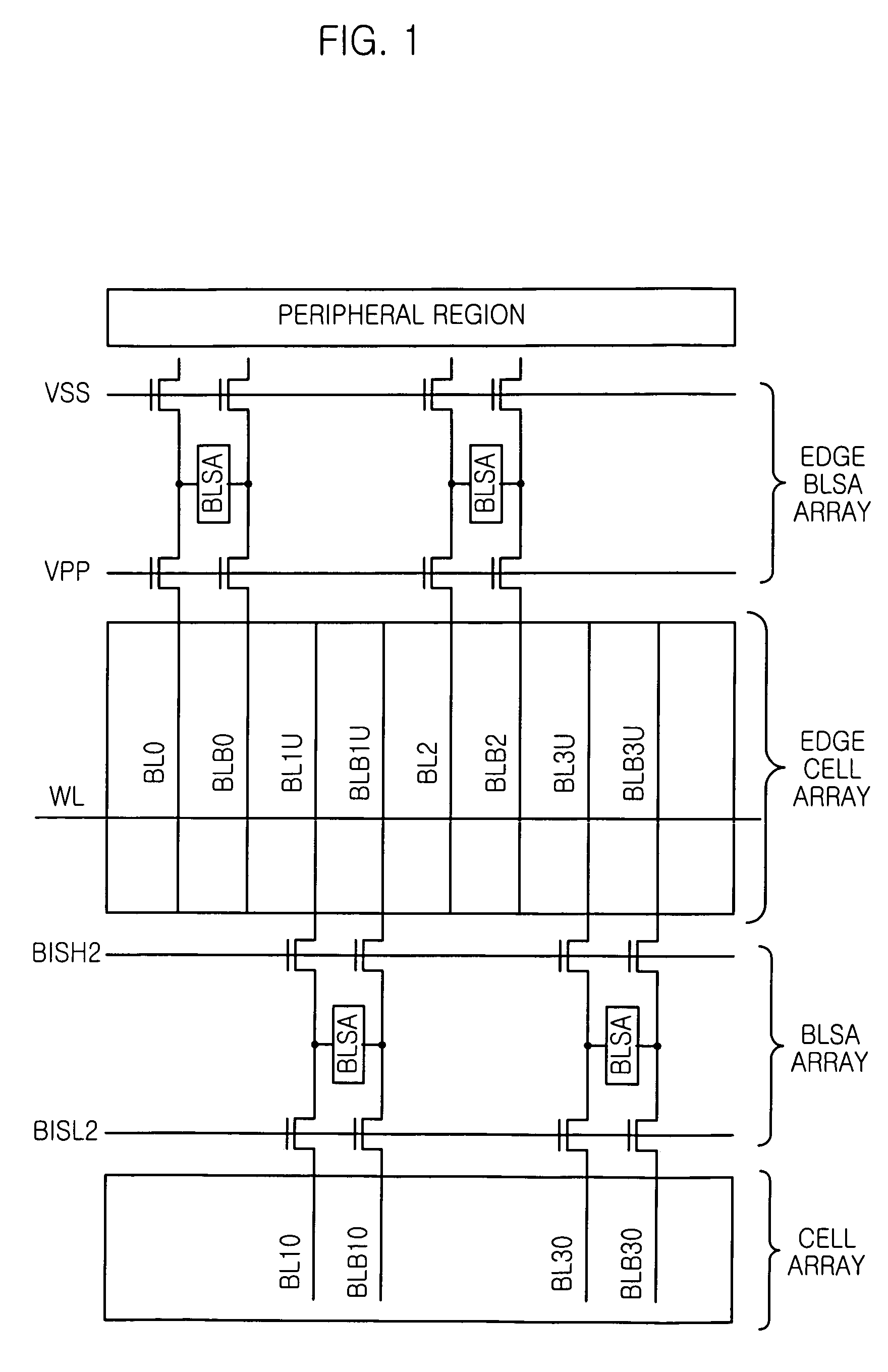
[0030]FIG. 1 is a block diagram showing a structure of a general semiconductor memory device.
[0031]In general, a cell area of the semiconductor memory device is generally divided into a plurality of cell array blocks.
[0032]Referring to FIG. 1, each of the cell array blocks includes a plurality of cell arrays, bit line sense amplifiers (BLSAs) disposed between the cell arrays, and edge BLSA arrays disposed at upper and lower edges. One cell array includes a plurality of cell columns, each of which includes memory cells sharing a bit line pair. Also, one bit line sense amplifier array includes a plurality of bit line sense amplifiers.
[0033]A structure that one bit line sense amplifier array manages the upper and lower cell arrays is called a “shared sense amplifier structure”. In the shared sense amplifier structure, one bit line sense amplifier is connected to a bit line pair (an upper bit line pair) of a cell column contained in an upper cell array through an upper bit line select s...
embodiment 2
[0053]FIGS. 6 and 7 are diagrams showing a structure of a semiconductor memory device in accordance with a second embodiment of the present invention. This embodiment is also applied to a DRAM having the shared sense amplifier structure.
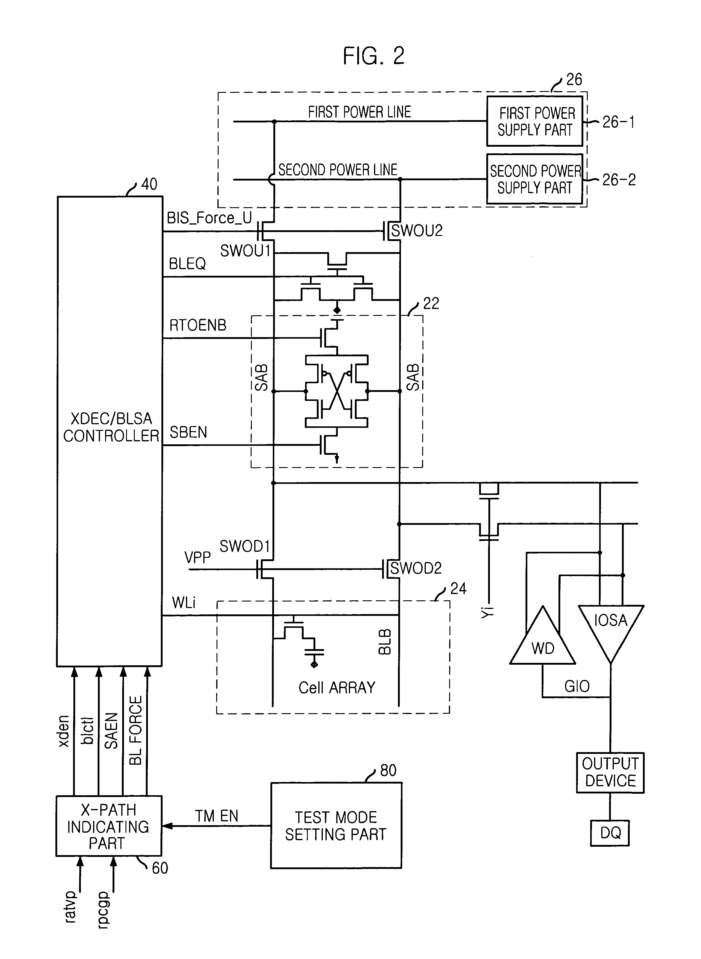
[0054]Referring to FIGS. 6 and 7, the semiconductor memory device includes a plurality of cell arrays. An edge bit line sense amplifier 22 amplifies data of some cell columns 24 among edge cell arrays, and a semi-edge bit line sense amplifier 32 amplifies data of other cell columns 34 among the cell arrays. A power supply part 26 supplies a predetermined voltage to the edge bit line sense amplifier 22, and a power transfer unit 38 transfers the voltage to the semi-edge bit line sense amplifier 32.
[0055]The power supply part 26 includes a first power supply switch SWOU1 for supplying a voltage to a bit line of the edge bit line sense amplifier 32, and a second power supply switch SWOU2 for supplying a voltage to a complementary bit line of the edge bi...
embodiment 3
[0069]In this embodiment, under the same structure of FIG. 2 in accordance with the first embodiment of the present invention, a new bit line sense amplifier including the first power supply part 26-1, the second power supply part 26-2, the first power supply switch SWOU1 and the second power supply switch SWOU2 can be defined. Since a detailed operation is equal to that of the first embodiment, a description thereof will be omitted.
PUM
 Abstract
Description
Claims
Application Information
 - R&D
- Intellectual Property
- Life Sciences
- Materials
- Tech Scout
- Unparalleled Data Quality
- Higher Quality Content
- 60% Fewer Hallucinations
Browse by: Latest US Patents, China's latest patents, Technical Efficacy Thesaurus, Application Domain, Technology Topic, Popular Technical Reports.
© 2025 PatSnap. All rights reserved.Legal|Privacy policy|Modern Slavery Act Transparency Statement|Sitemap|About US| Contact US: help@patsnap.com