
Process for forming microstructures

a microstructure and forming technology, applied in the field of forming microstructures, can solve the problems of not being able to achieve the effect of extending the structural stability of the structure, unable to generally be done through both the photoresist and the primary metal, and not being able to remove the photoresist first before the machining of the primary metal

Active Publication Date: 2007-09-18
FORMFACTOR INC
View PDF6 Cites 37 Cited by
  • Summary
  • Abstract
  • Description
  • Claims
  • Application Information

AI Technical Summary

Benefits of technology

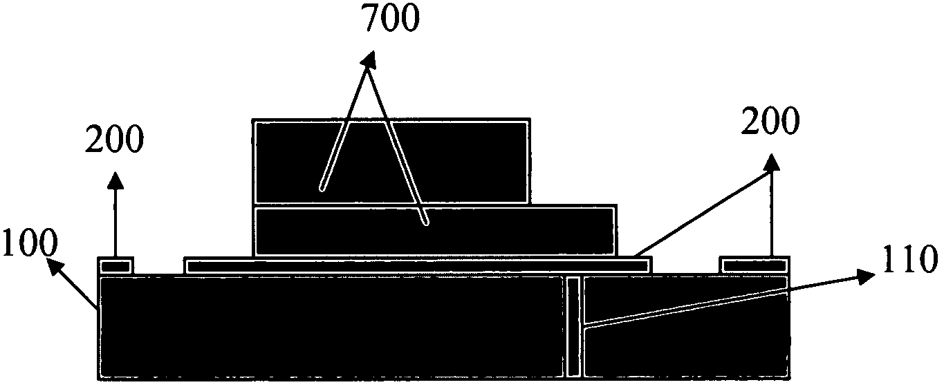
[0007]The present invention solves the above-described deficiencies by providing that the secondary metal is not plated over the entirety of the substrate's structured area. Instead the secondary metal is only plated in an area immediately surrounding the primary metal structure so that it lends its structural stability to the primary metal structure, but does not cause undue stress on the substrate. The present invention creates “islands” of secondary (sacrificial) metal, where it is needed for mechanical stability and the creation of structural overhangs instead of requiring the secondary metal to be formed in the entire area encompassing all structural metal regions on the substrate.

Problems solved by technology

Machining cannot generally be done through both the photoresist and the primary metal because the photoresist is relatively weak mechanically and may not adequately support the primary metal from damage due to the largely lateral forces encountered in the mechanical machining process (which may include machining, grinding, lapping, polishing, chemo-mechanical polishing, electric discharge machining, or any other commonly encountered machining process.
Likewise, the photoresist may not be removed first before the machining of the primary metal because of the likelihood of substantial damage to the primary metal structure, such as the tearing or ripping off of portions of the structure that are not laterally supported.
However, significant problems arise using this method when multiple or very laterally large microstructures are built on a single substrate, such as when manufacturing semiconductor testing probe heads.
This causes two related problems: 1) it becomes difficult or impossible to machine the different layers to a uniform thickness and 2) it becomes difficult or impossible to perform the lithography because micro-lithography requires a planar surface.
Several different techniques have been used or suggested to address this problem, however, each has its deficiencies.
However, during subsequent processing, such as photoresist curing, the applied heat may cause the secondary metal to become “stressy” (meaning to apply film stress relative to the substrate) thus the warping is not prevented.
However, the thickness of the substrate necessary to withstand the stress of the secondary metal may be impractical.
Additionally, the film stress (which is most often, though not necessarily, tensile in nature) causes mechanical failure at or near the substrate / metal interface, including both delamination and bulk fracture of the ceramic.

Method used


Image

  • Process for forming microstructures
  • Process for forming microstructures
  • Process for forming microstructures

Examples


Embodiment Construction

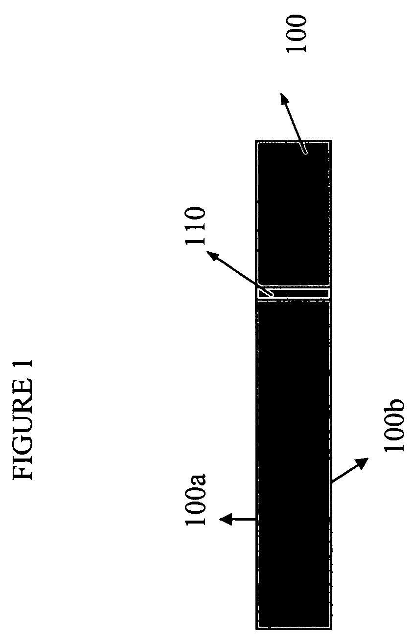
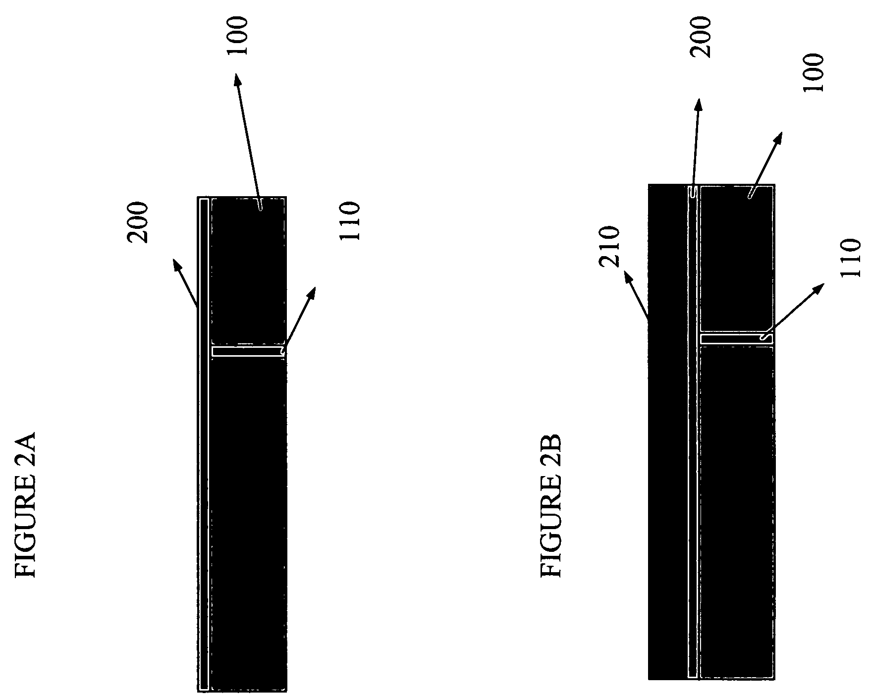
[0014]FIG. 1 shows a starting material on which to build the microstructure. The substrate 100 may be any type of substrate, including semiconductors such as silicon, germanium and gallium arsenide, ceramics such as alumina, aluminum, nitride low temperature cofired ceramics (LTCC) and high temperature cofired ceramics (HTCC), metals or glasses. In an embodiment of the present invention, microstructures such as springs used in testing semiconductor devices may be built on the substrate 100. In that case, the substrate 100 may be a Low Temperature Co-fired Ceramic (LTCC) substrate with built in vias 110 such that electricity may be conducted from one face 100a of the substrate 100 to the other face 100b of the substrate 100 by way of the vias 110. In an embodiment of the present invention, the vias 110 are made from gold, but any other conductor such as copper or platinum may be used. The ceramic may also contain electrical redistribution conductors, making it an electrical “space tr...


PUM


Abstract

The present invention relates to a process for forming microstructures on a substrate. A plating surface is applied to a substrate. A first layer of photoresist is applied on top of the plating base. The first layer of photoresist is exposed to radiation in a pattern to render the first layer of photoresist dissolvable in a first pattern. The dissolvable photoresist is removed and a first layer of primary metal is electroplated in the area where the first layer of photoresist was removed. The remainder of the photoresist is then removed and a second layer of photoresist is then applied over the plating base and first layer of primary metal. The second layer of photoresist is then exposed to a second pattern of radiation to render the photoresist dissolvable and the dissolvable photoresist is removed. The second pattern is an area that surrounds the primary structure, but it does not entail the entire substrate. Rather it is an island surrounding the primary metal. The exposed surface of the secondary metal is then machined down to a desired height of the primary metal. The secondary metal is then etched away.

Description

RELATED APPLICATION[0001]This application is a Continuation-In-Part of application Ser. No. 11 / 019,912 titled “Process for Forming Microstructures” filed Dec. 21, 2004.BACKGROUND[0002]The formation of micromechanical structures using photolithography and sacrificial layers is known in the art. The present invention is an improvement to the technology disclosed in U.S. Pat. No. 5,190,637 to Gluckel, titled“Formation of Microstructures by Multiple Level Deep X-ray Lithography with Sacrificial Metal Layers,”(“the '637 patent”), which is incorporated herein by reference. In the '637 patent, microstructures are built in several steps. First, a layer of photoresist capable of exposure by radiation is applied to a plating base. The photoresist is then exposed to radiation using a mask. The mask allows the radiation to only “expose” a certain defined area of the photoresist. Subsequent developing removes photoresist selective to the exposure creating a cavity that replicates the plan of the...

Claims


Application Information

Patent Timeline
Patent Type & Authority Patents(United States)
IPC IPC(8): H01L21/00H01L21/4763
CPCB81C1/00436B81C1/00666B81C2201/0107B81C2201/0197
Inventor TANG, WEILONGHSU, TSENG-YANGISMAIL, SALLEHTEA, NIM HAKKHOO, MELVIN BGARABEDIAN, RAFFINAMBURI, LAKSHIMIKANTH
Owner FORMFACTOR INC
Learn More