Semiconductor devices having field effect transistors
a field effect transistor and semiconductor technology, applied in semiconductor devices, strainers, kitchen equipment, etc., can solve the problems of limiting the size of planar transistors, requiring fast speed, and transistors continuing to become smaller
- Summary
- Abstract
- Description
- Claims
- Application Information
AI Technical Summary
Benefits of technology
Problems solved by technology
Method used
Image

Examples
Embodiment Construction
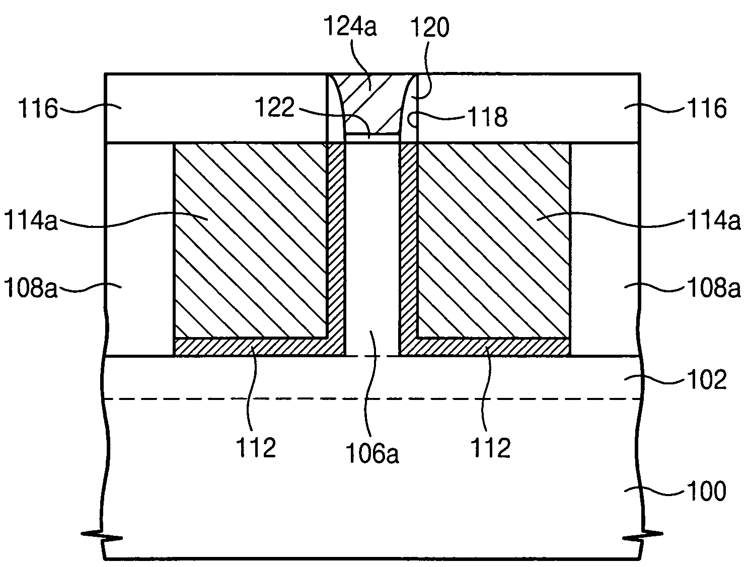
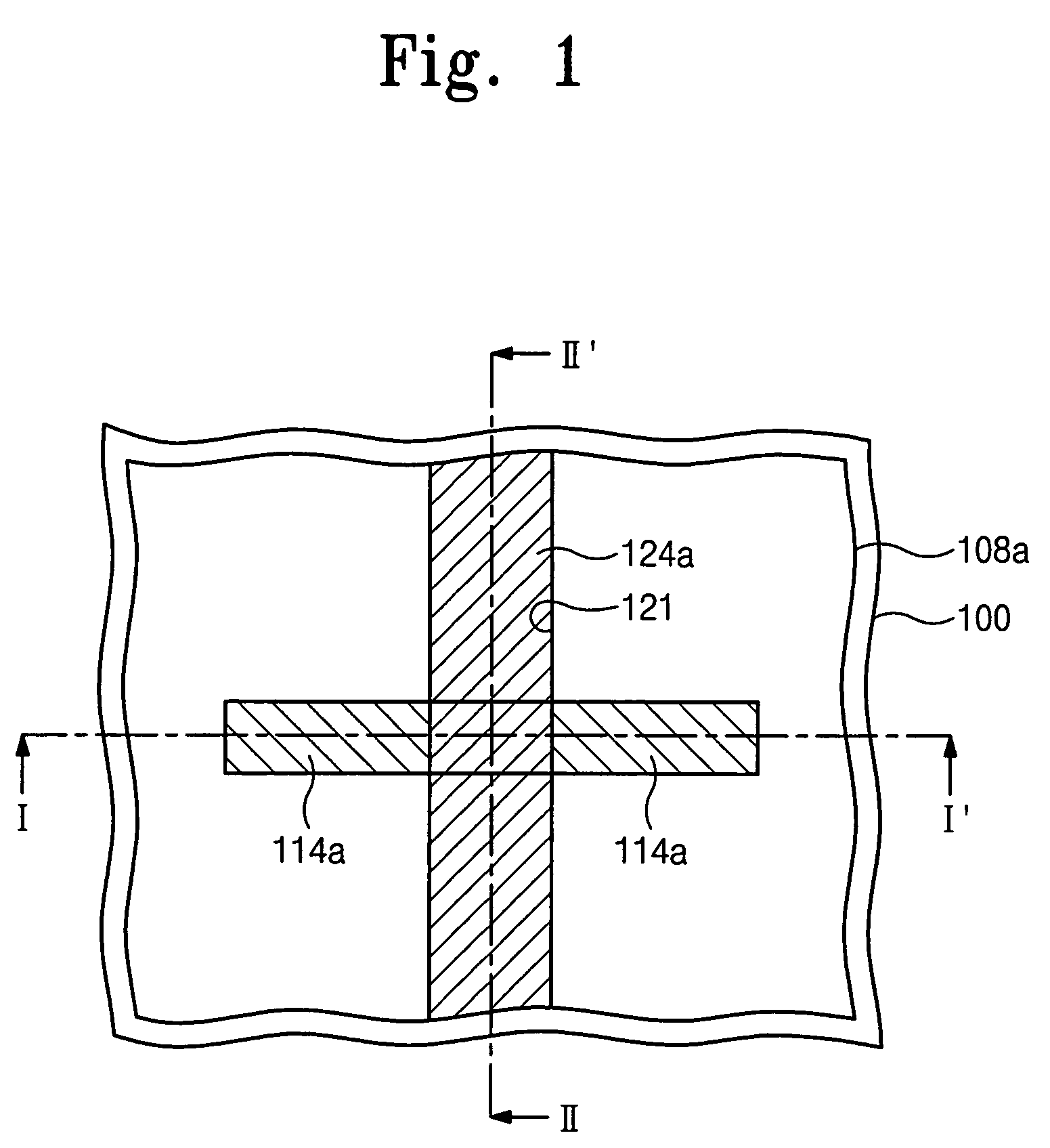
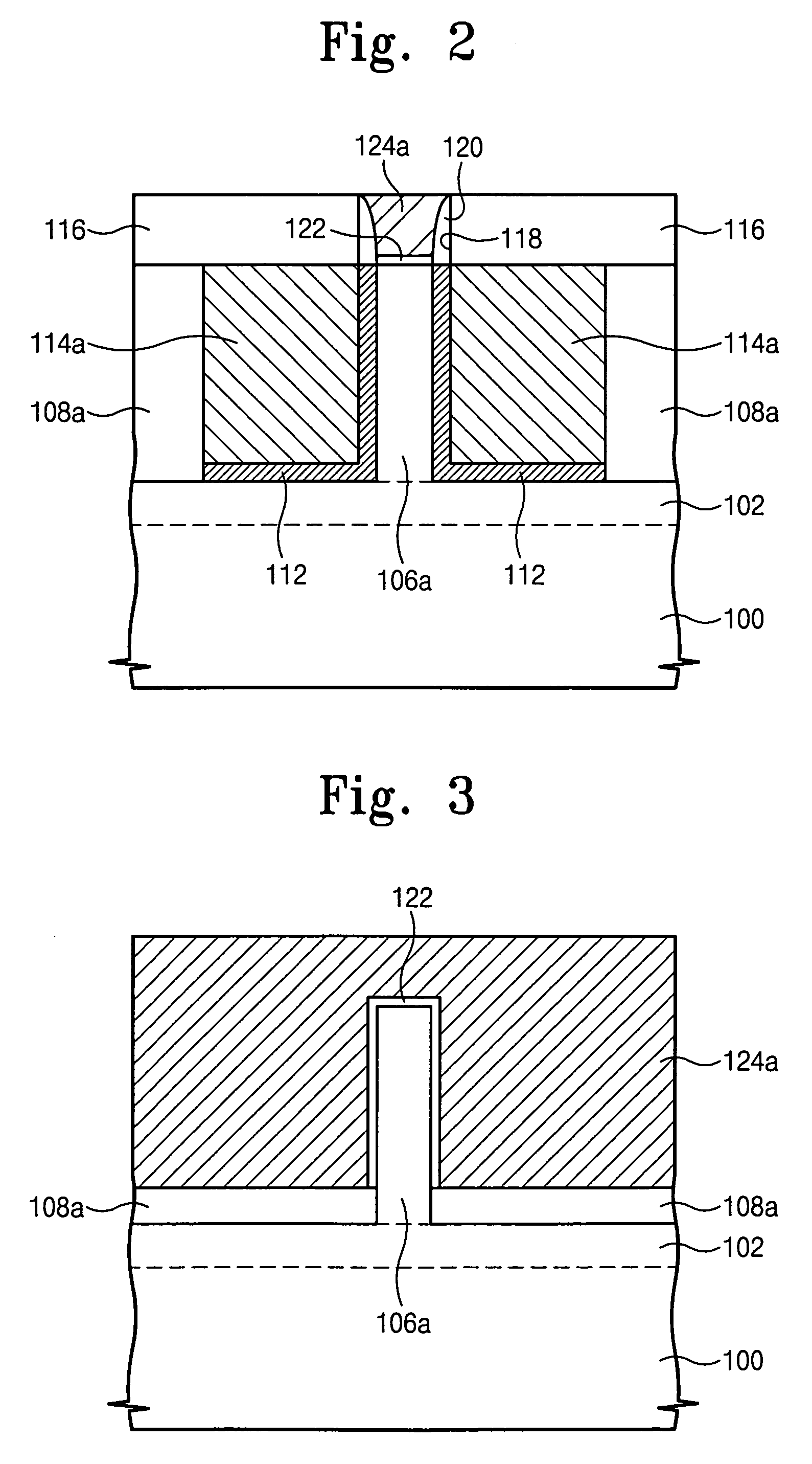
[0028]Referring to FIGS. 1, 2, and 3, a protruded channel pattern 106a is vertically extended from a substrate 100. The protruded channel pattern 106a has a pair of first sidewalls facing each other and a pair of second sidewalls facing each other. The first sidewalls may be perpendicular to the second sidewalls. A pair of in-situ doped epitaxial patterns 112 are formed on the first sidewalls of the protruded channel pattern 106a. The in-situ doped epitaxial pattern 112 covers the first sidewalls. The in-situ doped epitaxial pattern 112 is vertically protruded from the substrate 100 and is included in source / drain regions of a transistor. It is preferable that the substrate 100 be a silicon substrate. It is preferable that the protruded channel pattern 106a is formed with a single crystalline silicon. The protruded channel pattern 112 may be a part of the substrate 100. The in-situ doped epitaxial pattern 112 is a doped semiconductor layer by performing, for example, an in-situ dope...
PUM
 Abstract
Description
Claims
Application Information
 - R&D
- Intellectual Property
- Life Sciences
- Materials
- Tech Scout
- Unparalleled Data Quality
- Higher Quality Content
- 60% Fewer Hallucinations
Browse by: Latest US Patents, China's latest patents, Technical Efficacy Thesaurus, Application Domain, Technology Topic, Popular Technical Reports.
© 2025 PatSnap. All rights reserved.Legal|Privacy policy|Modern Slavery Act Transparency Statement|Sitemap|About US| Contact US: help@patsnap.com