Method and apparatus for determining sensing timing of flash memory

a technology of flash memory and sensing timing, which is applied in the direction of digital storage, static storage, instruments, etc., can solve the problems of time-consuming and laborious tuning of the threshold voltage of the reference cell, the inability of the corresponding word line to access normal cells, and the inability to efficiently adjust the threshold voltage of so many reference cells

Active Publication Date: 2007-08-28
ELITE SEMICON MEMORY TECH INC
View PDF7 Cites 12 Cited by
  • Summary
  • Abstract
  • Description
  • Claims
  • Application Information

AI Technical Summary

Benefits of technology

[0011]The primary objective of the present invention is to provide a method for automatically determining a sensing time in a page buffer of normal cells in a memory cell array of a flash memory device and an apparatus performing the operation. The secondary objective of the present invention is to provide a method and an apparatus to eliminate the drifting of the threshold voltage of the reference cell during program or erase operations in a flash memory device.
[0012]In order to achieve the objectives, a method and an apparatus for determining a sensing time in a page buffer of normal cells in a memory cell array of a NAND flash memory device are disclosed. The apparatus of the present invention comprises a first reference bit line, a first current sink, a first reference page buffer, a second group of reference bit lines, a second current sink and a second reference page buffer. The first reference bit line is coupled between the first current sink and the first reference page buffer. The second group of reference bit lines are coupled between the second current sink and the second reference page buffer. Both the first and second current sinks are disposed out of the memory cell array where the normal cells and normal bit lines are located. Consequently, the drifting of the threshold voltage of the reference cells can be eliminated during program and erase operations. Each of the first and second current sinks provides the first and second reference bit lines paths to ground, respectively, and is located at the farthest end of the respective reference bit line from the respective reference page buffer.
[0013]In an embodiment, each of the first and second current sinks is implemented by a single reference cell, e.g., a NAND cell, whose control gate is connected to a reference word line. In another embodiment, each of the first and second current sinks comprises a plurality of fuse groups. Each fuse group is connected to a MOSFET in series, and the fuse groups are connected in parallel with a reference word line connected to each gate electrode of the MOSFETs. These fuses are used to tune the sink current. The reference word line of the current sink is isolated from the normal cell word lines. Accordingly, elimination of the drifting of the threshold voltages of the reference cells is enhanced during program and erase operations. Moreover, the apparatus of the present invention can further comprises a first reference shielding bit line to shield the first reference bit line and a second reference shielding bit line to shield the second reference bit line.

Problems solved by technology

However, this method will result in difficulty in efficiently adjusting the threshold voltages for so many reference cells.
However, if one of the reference cells fails, the corresponding word line fails to access normal cells.
However, in this design, tuning the threshold voltages of the reference cells is time-consuming, increasing production cost drastically and therefore not feasible.
Thus, the control of the sensing timing by the timer may fail if the RC (product of resistance and capacitance) of the bit line changes due to variation of the fabrication process.

Method used


Image

  • Method and apparatus for determining sensing timing of flash memory
  • Method and apparatus for determining sensing timing of flash memory
  • Method and apparatus for determining sensing timing of flash memory

Examples


Embodiment Construction

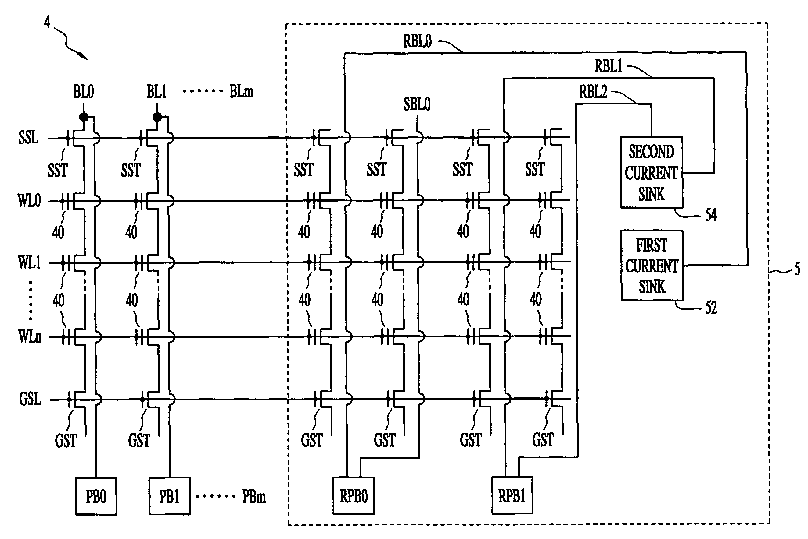
[0025]FIG. 4 illustrates a memory cell array 4 of a NAND flash memory device configured with the automatic sensing-time determining apparatus 5. The memory cell array 4 contains a string select line SSL, a ground source line GSL, a plurality of word lines (WL0-WLn) each coupling to a control gate of a plurality of normal cells 40, and a plurality of normal cell bit lines (BL0-BLm) each coupling to the respective string select transistor SST and coupling to the respective page buffer (PB0-PBm) thereof. The automatic sensing-time determining apparatus 5 comprises a first reference bit line RBL0, a second group of reference bit lines RBL1 and RBL2, a first current sink 52, a second current sink 54, a first reference page buffer RPB0 and a second reference page buffer RPB1. The first reference bit line RBL0 is coupled to the first current sink 52 and the first reference page buffer RPB0 at both ends thereof. The second group of reference bit lines RBL1 and RBL2 are coupled to the second...


PUM


Abstract

A method of automatically determining a sensing timing in a page buffer of a NAND flash memory device is disclosed, which includes the steps of discharging a first reference bit line, discharging a second reference bit line, determining a first control signal and determining a second control signal. To perform the method, an apparatus of automatically determining a sensing timing in a page buffer of a NAND flash memory device is also disclosed. The apparatus includes a first reference bit line, a first current sink, a first reference page buffer, the second reference bit line, a second current sink and a second reference page buffer. The first reference bit line is coupled to the first current sink and the first reference page buffer at both ends thereof. The second reference bit line is coupled to the second current sink and the second reference page buffer at both ends thereof.

Description

RELATED U.S. APPLICATIONS[0001]Not applicable.STATEMENT REGARDING FEDERALLY SPONSORED RESEARCH OR DEVELOPMENT[0002]Not applicable.REFERENCE TO MICROFICHE APPENDIX[0003]Not applicable.FIELD OF THE INVENTION[0004]The present invention relates to a method for determining a sensing timing and an apparatus performing the same, more particularly, to a method and an apparatus for automatically determining a sensing timing in a page buffer of normal cells in a memory cell array of a flash memory device. The sensing timing determines the activation of the control signals to start the operation of read or verifications in the flash memory device.BACKGROUND OF THE INVENTION[0005]In a NAND flash memory, the data stored in a cell is read out through the page buffer. The page buffer also serves program verification and erase verification that function as a read operation. Page buffers appear in a variety of designs. FIG. 1 is one design of page buffer, which is published in “A 3.3 V 32 Mb NAND fl...

Claims


Application Information

Patent Timeline
Patent Type & Authority Patents(United States)
IPC IPC(8): G11C11/34
CPCG11C16/32G11C16/3436G11C16/3445G11C16/3459G11C16/28
Inventor CHEN, CHUNG ZEN
Owner ELITE SEMICON MEMORY TECH INC
Why Eureka
Try Eureka