
Liquid crystal display device with a bridge wiring member with an electric field weaker than that created in minute domains above the pixel electrode

a technology of pixel electrodes and wiring members, applied in static indicating devices, instruments, non-linear optics, etc., to achieve the effect of enhancing display quality and reducing display irregularities

Active Publication Date: 2007-08-21
JAPAN DISPLAY CENTRAL CO LTD
View PDF7 Cites 5 Cited by
  • Summary
  • Abstract
  • Description
  • Claims
  • Application Information

AI Technical Summary

Benefits of technology

[0013]An object of this invention is to provide a liquid crystal display device which can solve the above problem and reduce display irregularity caused by application of a mechanical shock to enhance the display quality.
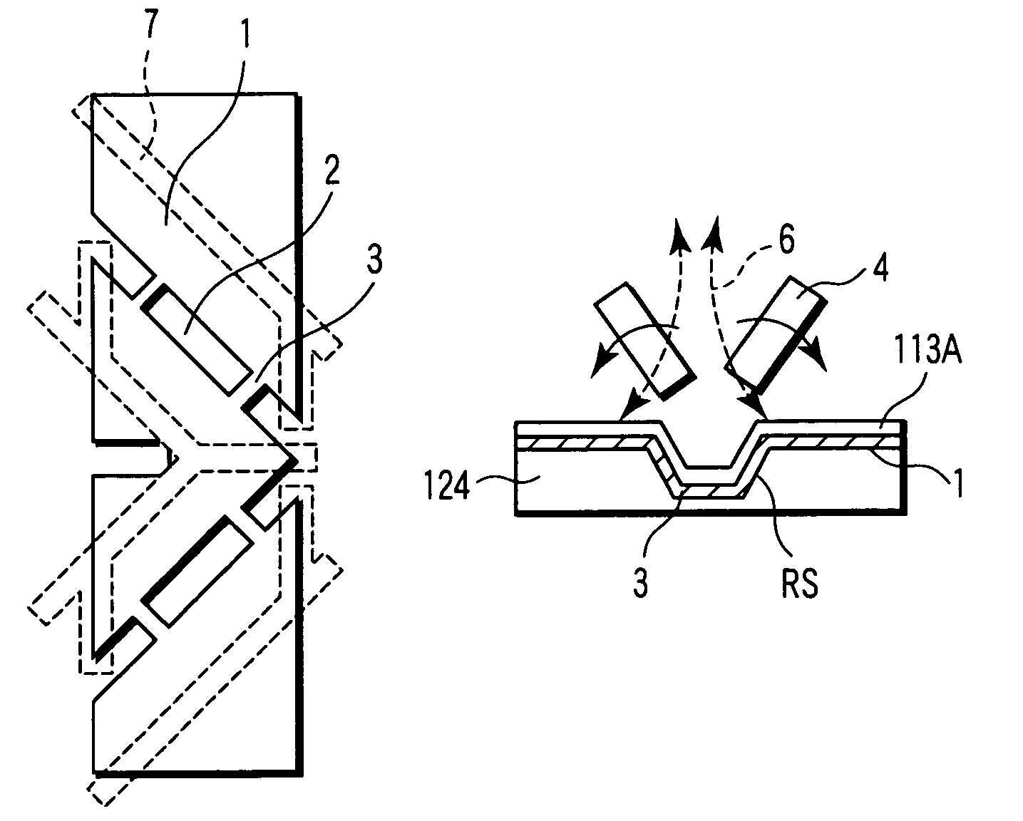
[0016]In the above liquid crystal display devices, the bridge-wiring member is configured to make an electric field created in the part of the pixel area located on the bridge-wiring member weaker than an electric field created in the minute domains when the potential difference is applied between the first and second electrodes. As a result, the electric field on the bridge-wiring member can be made substantially equivalent to the electric field on the void space. Thus, the tilt directions (directors) of the liquid crystal molecules near the bridge-wiring member can be set equal to that near the void space. Since the electric fields on the bridge-wiring member and the void space are controlled to be equivalent distortion, the original state can be rapidly restored even if the alignment of the liquid crystal molecules is made irregular upon application of a mechanical shock.
[0017]Further, for example, the structure of the first substrate can be obtained by separating the bridge-wiring member further apart from the second electrode than the conductor in the first substrate, adding an insulating body having a smaller dielectric constant than the liquid crystal layer on the bridge-wiring member or using a combination of the above methods. In practice, the bridge-wiring member separated further apart from the second electrode than the conductor in the first substrate can be easily attained by, for example, forming an insulating layer on the first substrate as an underlying layer of the conductor and bridge-wiring member, and forming in the insulating material layer a concave portion that receives the bridge wiring portion to set the bridge-wiring member in position lower than the conductor.

Problems solved by technology

Thus, the same problem occurs when a bridge-wiring member is provided as wirings that electrically connect the sub-pixel electrode segments to set them to the same potential without requiring a redundant wiring space.

Method used


Image

  • Liquid crystal display device with a bridge wiring member with an electric field weaker than that created in minute domains above the pixel electrode
  • Liquid crystal display device with a bridge wiring member with an electric field weaker than that created in minute domains above the pixel electrode
  • Liquid crystal display device with a bridge wiring member with an electric field weaker than that created in minute domains above the pixel electrode

Examples


Embodiment Construction

[0037]There will now be described an active matrix type liquid crystal display device according to a first embodiment of this invention with reference to the accompanying drawings. The liquid crystal display device is configured as a liquid crystal display panel 100 containing a drive circuit, for example.

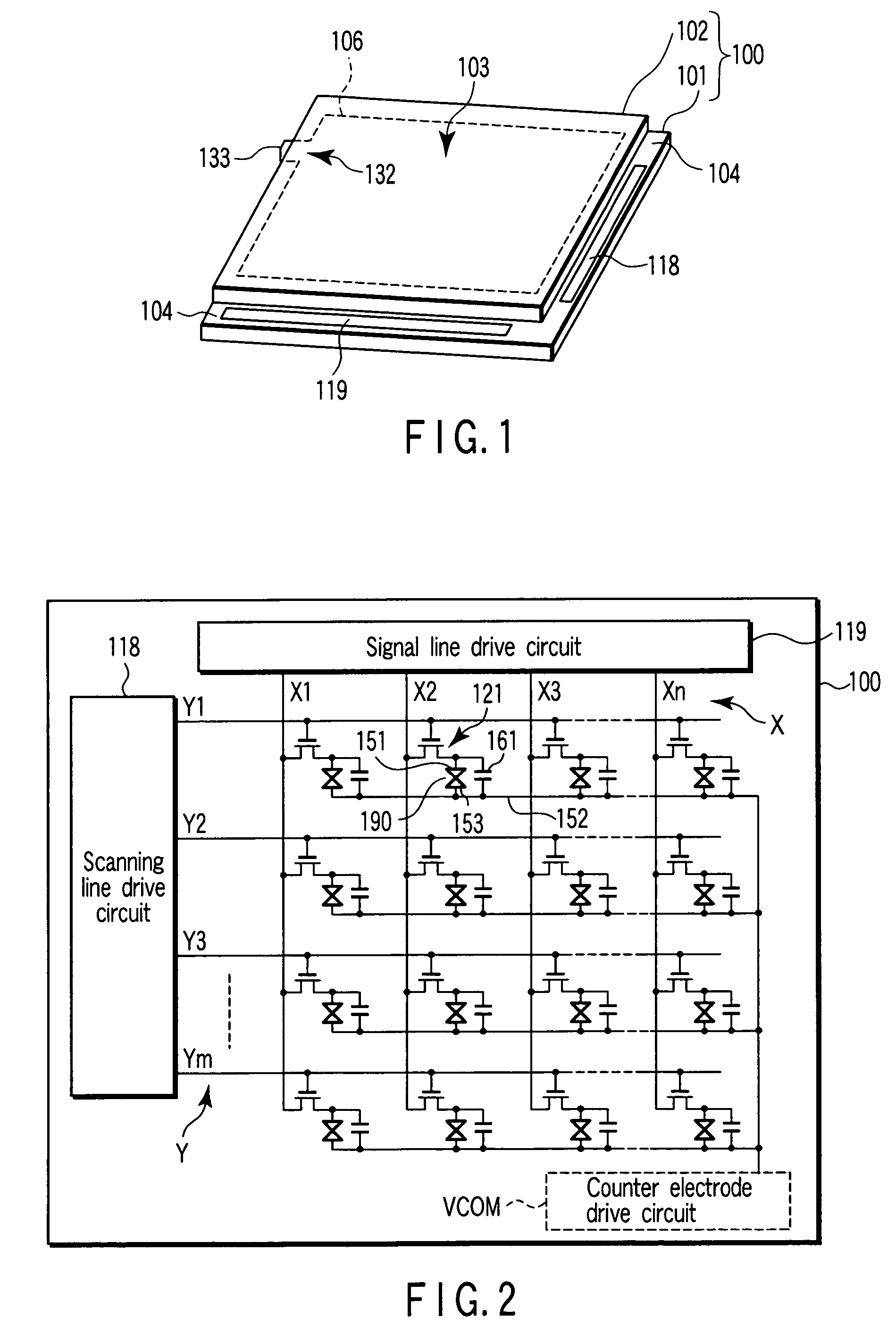
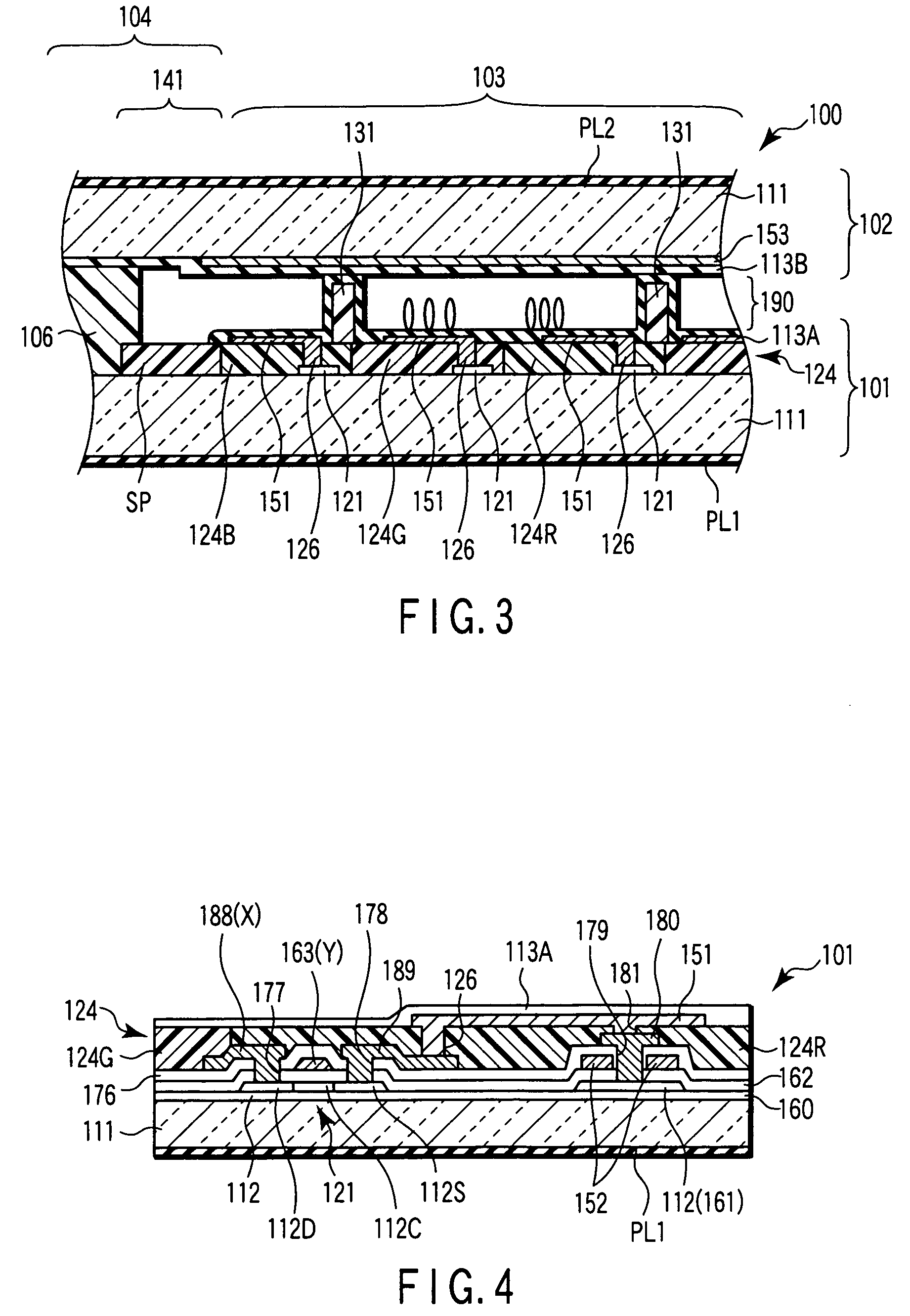
[0038]FIG. 1 shows the appearance of the liquid crystal display panel 100, FIG. 2 schematically shows the circuit configuration of the liquid crystal display panel 100 shown in FIG. 1, FIG. 3 schematically shows the cross section of the liquid crystal display panel 100 shown in FIG. 1, and FIG. 4 shows the cross sectional structure of an array substrate of FIG. 3 in detail.

[0039]As shown in FIG. 1, the liquid crystal display panel 100 includes an array substrate 101, a counter electrode 102 which faces the array substrate 101, and a liquid crystal layer 190 containing a liquid crystal composition held between the array substrate 101 and the counter electrode 102. The array substrat...


PUM

PropertyMeasurementUnit
thicknessaaaaaaaaaa
dielectric constantaaaaaaaaaa
depthaaaaaaaaaa

Abstract

A liquid crystal display device includes an array substrate having a pixel electrode formed of a conductor, a counter substrate having a counter electrode facing the pixel electrode, and a liquid crystal layer held between the substrates and containing liquid crystal molecules set in a vertical alignment with respect to the substrates. The pixel electrode had a void space located in the conductor to provide minute domains between which different directors of the liquid crystal molecules are obtained when a potential difference is applied between the array and counter electrodes, and a bridge-wiring member interconnecting adjacent parts of the conductor in the void space, and the bride-wiring member is configured to make an electric field created in a part of the pixel area located on the bridge-wiring member weaker than that created in the minutes domains according to the potential difference.

Description

CROSS-REFERENCE TO RELATED APPLICATIONS[0001]This application is based upon and claims the benefit of priority from the prior Japanese Patent Application No. 2003-006980, filed Jan. 15, 2003, the entire contents of which are incorporated herein by reference.BACKGROUND OF THE INVENTION[0002]1. Field of the Invention[0003]This invention relates to a liquid crystal display device wherein a liquid crystal layer is held between a pair of electrode substrates and more particularly to a liquid crystal display device whose a liquid crystal layer is divided into a plurality of domains between which liquid crystal molecules are set in different tilt directions.[0004]2. Description of the Related Art[0005]Liquid crystal display devices are applied in various fields of OA equipments, information terminals, watches, televisions and the like because of their characteristics of lightness, thinness and low power consumption. Particularly, an active matrix type liquid crystal display panel has an ex...

Claims


Application Information

Patent Timeline
Patent Type & Authority Patents(United States)
IPC IPC(8): G02F1/1337G02F1/133G02F1/1333G02F1/1343
CPCG02F1/134336G02F1/133707G02F1/133
Inventor YAMAGUCHI, TAKESHININOMIYA, KISAKOKAWATA, YASUSHIHISATAKE, YUZOFUJIYAMA, NATSUKOMURAYAMA, AKIO
Owner JAPAN DISPLAY CENTRAL CO LTD
Learn More