Broadband modulation PLL, and modulation factor adjustment method thereof
a modulation factor and wide band technology, applied in the direction of modulation, pulse automatic control, and varying frequency control of electrical components, can solve the problems of high manufacturing cost, deformation of noise characteristics, and increased time consumption, and achieve low cost and good modulation accuracy
- Summary
- Abstract
- Description
- Claims
- Application Information
AI Technical Summary
Benefits of technology
Problems solved by technology
Method used
Image

Examples
first embodiment
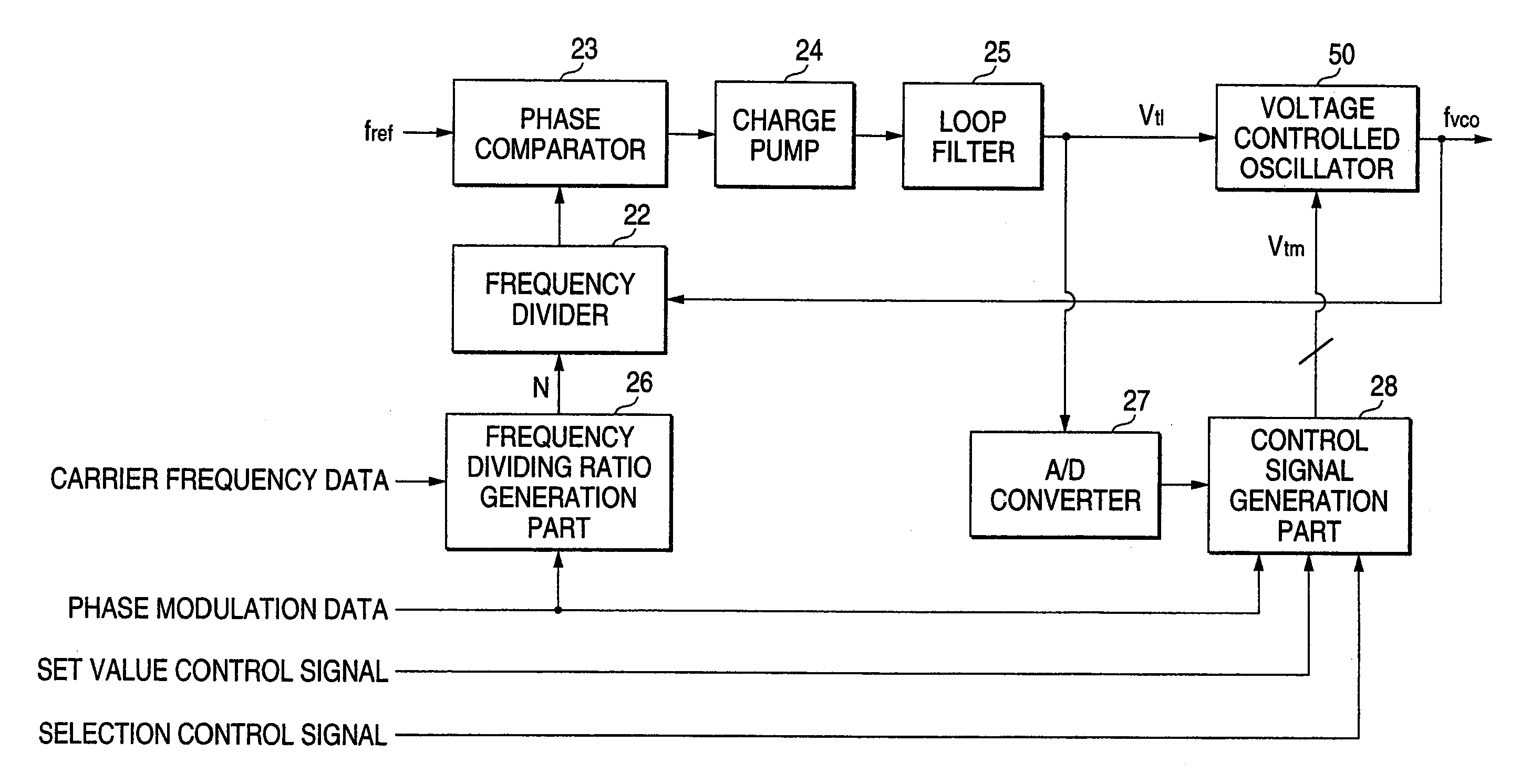
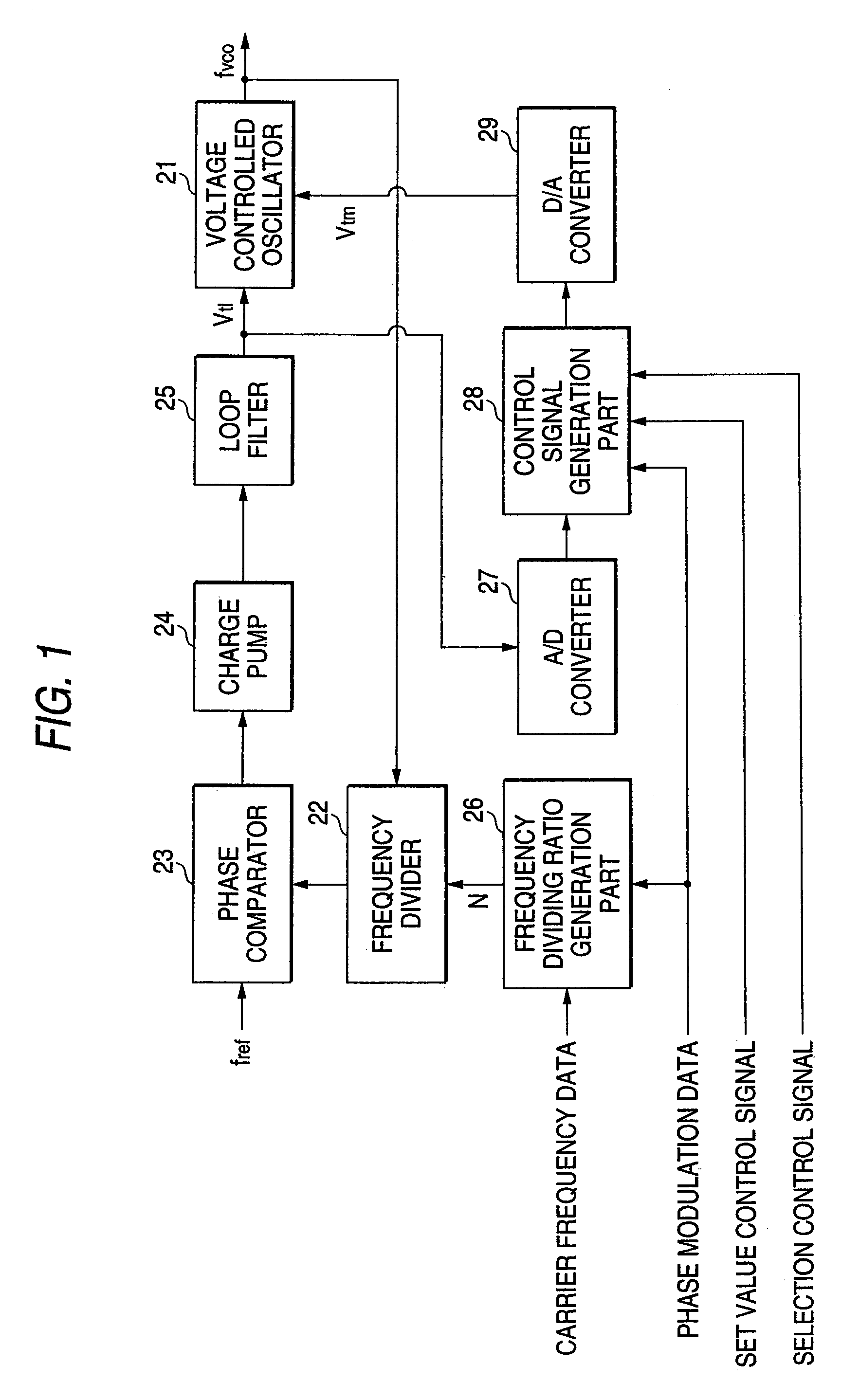
[0059]FIG. 1 is a schematic configuration diagram showing a wide band modulation PLL for describing a first embodiment of the present invention. In FIG. 1, a wide band modulation PLL according to the first embodiment comprises a PLL having a voltage controlled oscillator (hereinafter VCO) 21 with two control voltage terminals for PLL (input voltage Vtl) and modulation signal input (input voltage Vtm), a frequency divider 22 for dividing a frequency of an output signal of the VCO 21, a phase comparator 23 for comparing a phase of a reference signal with a phase of an output signal of the frequency divider 22 and outputting a signal according to a phase difference, a charge pump 24 for converting an output signal of the phase comparator 23 into a control signal of the VCO 21 and a loop filter 25 for smoothing an output signal of the charge pump 24 and outputting a control voltage Vtl to the control voltage terminal for PLL of the VCO 21.
[0060]Further, the wide band modulation PLL acco...
second embodiment
[0093]FIG. 6 is a schematic configuration diagram showing a wide band modulation PLL for describing a second embodiment of the present invention. The same numerals are attached to portions overlapping with FIG. 1 described in the first embodiment.
[0094]In FIG. 6, the wide band modulation PLL according to the second embodiment includes a direct digital synthesizer (hereinafter DDS) 40 and differs from that of the first embodiment in that a point at which phase modulation is performed is two points of the DDS 40 and a VCO 21.
[0095]The DDS 40 is adapted for directly outputting a result of numerical operation through a built-in D / A converter etc. and as shown in FIG. 6, based on carrier frequency data and phase modulation data, numerical calculation can be performed to output a carrier signal and a modulation signal. Since modulation in the DDS 40 is similar to frequency dividing ratio modulation of the first embodiment, modulation factor adjustment and calculation of a modulation sensi...
third embodiment
[0098]FIG. 7 is a schematic configuration diagram showing a wide band modulation PLL for describing a third embodiment of the present invention. The same numerals are attached to portions overlapping with FIG. 1 described in the first embodiment.
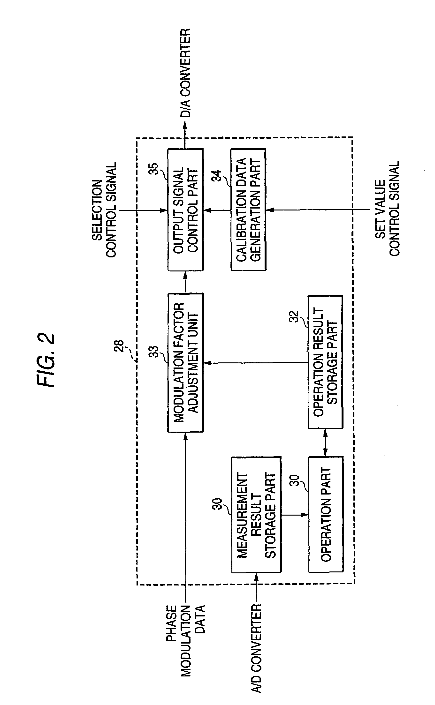
[0099]In the present embodiment, a signal outputted from a control signal generation part 28 is inputted to a VCO 50 in a state of a digital signal without making D / A conversion. The VCO 50 has a switch and small capacitance in parallel with an LC resonator, and performs an action similar to that of the VCO 21 shown in FIG. 3 by changing the total capacitance value by controlling this switch through the digital signal. A method of adjustment and measurement of a modulation sensitivity is similar to that of the first embodiment.
[0100]FIG. 8 is a principle diagram showing one example of a VCO used in the wide band modulation PLL according to the third embodiment. As shown in FIG. 8, in the VCO 50, n Cvm(1) to Cvm(n) in which capacitance is var...
PUM
 Abstract
Description
Claims
Application Information
 - R&D
- Intellectual Property
- Life Sciences
- Materials
- Tech Scout
- Unparalleled Data Quality
- Higher Quality Content
- 60% Fewer Hallucinations
Browse by: Latest US Patents, China's latest patents, Technical Efficacy Thesaurus, Application Domain, Technology Topic, Popular Technical Reports.
© 2025 PatSnap. All rights reserved.Legal|Privacy policy|Modern Slavery Act Transparency Statement|Sitemap|About US| Contact US: help@patsnap.com