Active matrix organic electro luminescence display device and manufacturing method for the same
a technology of active matrix and electroluminescence display, which is applied in the direction of electroluminescent light sources, transistors, electric lighting sources, etc., can solve the problems of increasing manufacturing time and cost according to the related arts, affecting the effect of the effect of the effect of the effect of the aperture ratio, reducing the number of masks needed, and increasing the storage capacitance of the storage capacitor
- Summary
- Abstract
- Description
- Claims
- Application Information
AI Technical Summary
Benefits of technology
Problems solved by technology
Method used
Image

Examples
Embodiment Construction
[0033]Reference will now be made in detail to the illustrated embodiment of the present invention, which is illustrated in the accompanying drawings.
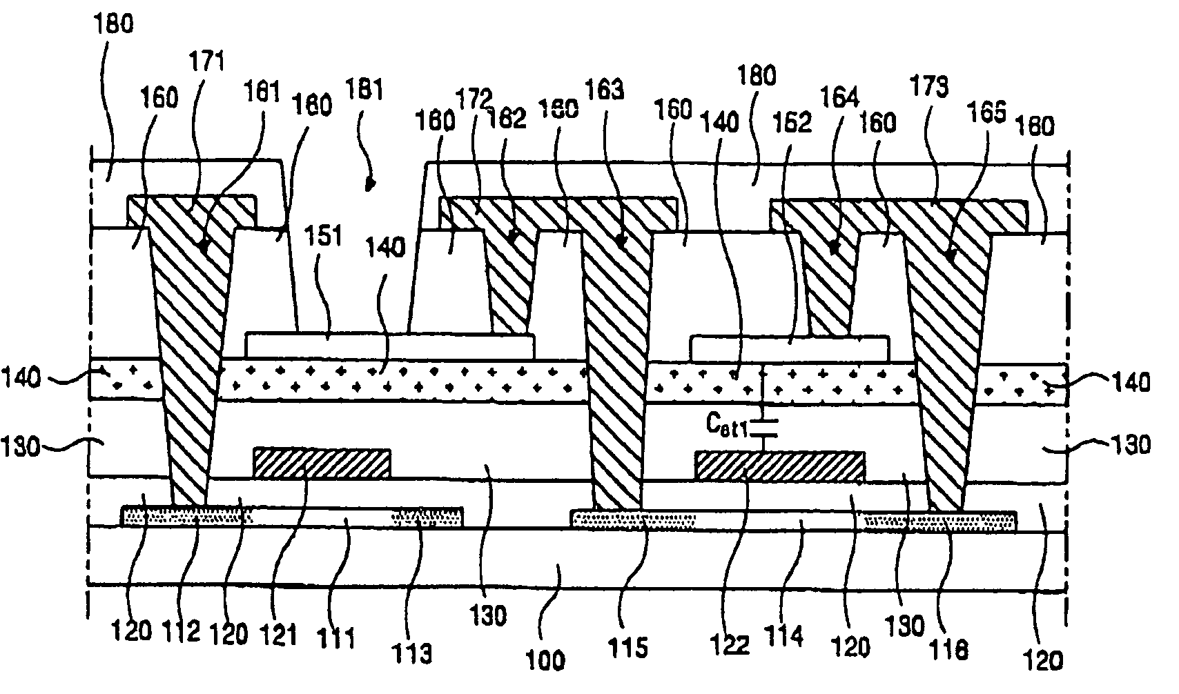
[0034]FIG. 5 is a cross-sectional view of an active matrix organic electro luminescent display device according to a first embodiment of the present invention. In FIG. 5, a polycrystalline silicon layer 111, 112, 113, 114, 115 and 116 is formed on a transparent insulating substrate 100. The polycrystalline silicon layer 111, 112, 113, 114, 115 and 116 is divided into two regions that one has an active layer 111, a first source region 112 and a first drain region 113 and the other has an active layer 114, a second drain region 115 and a second source region 116. Impurities are doped onto the first source and drain regions 112 and 113 and the second source and drain regions 116 and 115. A gate insulating layer 120 is formed on the polycrystalline silicon layer 111, 112, 113, 114, 115 and 116. First and second gate electrodes 121 and 122 a...
PUM
 Abstract
Description
Claims
Application Information
 - R&D
- Intellectual Property
- Life Sciences
- Materials
- Tech Scout
- Unparalleled Data Quality
- Higher Quality Content
- 60% Fewer Hallucinations
Browse by: Latest US Patents, China's latest patents, Technical Efficacy Thesaurus, Application Domain, Technology Topic, Popular Technical Reports.
© 2025 PatSnap. All rights reserved.Legal|Privacy policy|Modern Slavery Act Transparency Statement|Sitemap|About US| Contact US: help@patsnap.com