
Method to adjust the signal level of an active pixel and corresponding active pixel

a signal level and signal technology, applied in the field of method for adjusting the signal level of an active pixel and an active pixel, can solve problems such as signal attenuation

Active Publication Date: 2007-05-29
SEMICON COMPONENTS IND LLC
View PDF5 Cites 57 Cited by
  • Summary
  • Abstract
  • Description
  • Claims
  • Application Information

AI Technical Summary

Benefits of technology

[0006]It is an object of the present invention to provide a method to overcome signal attenuation in active pixels, as well as to provide an active pixel which does not present the problem of large signal attenuation.
[0007]This object is accomplished by introducing a capacitor element with two nodes in an active pixel. Therefore, an active pixel according to the present invention, comprises a sensor circuit for collecting radiation induced charges and transducing them to a measurement signal corresponding to the amount of charge collected, and a capacitor element with two nodes. The pixel's signal is present on a first node of the capacitor element (it may e.g. be stored there), and the signal level is changed by changing the voltage on the other node of the capacitor element. The active pixels may be of various types, e.g. as used for synchronous detection of light. The capacitor element is clocked, i.e. driven by a pulsed signal. The pulse on the capacitor element can raise the reset level at the output by, for instance, about 1 to 2 Volts, thus restoring a large signal swing.
[0015]The present invention furthermore describes a method for reading out an active pixel according to the present invention, which method can reduce signal attenuation.
[0022]Preferably, the array further comprises a circuit for controlling the timing of sampling and pre-charging of all the active pixels of the array at the same time. The capacitor element is clocked, i.e. driven by a pulsed signal. The array may also comprise a read-out circuit connected to the capacitor element(s), for reading out the measurement signal present or stored on the capacitor element(s). A pulse may be applied to the capacitor element which can raise the reset level at the output by, for instance, about 1 to 2 Volts, thus restoring a large signal swing.

Problems solved by technology

This known active pixel has the disadvantage that, due to the presence of several transistors, more specifically the reset transistor, and each of the buffer transistors, there are different MOSFET threshold voltage drops in the circuit, which cause signal attenuation.

Method used


Image

  • Method to adjust the signal level of an active pixel and corresponding active pixel
  • Method to adjust the signal level of an active pixel and corresponding active pixel
  • Method to adjust the signal level of an active pixel and corresponding active pixel

Examples


Embodiment Construction

[0033]The present invention will be described with respect to particular embodiments and with reference to drawings, but the invention is not limited thereto but only by the claims. The drawings described are only schematic and are non-limiting. In the following description it should be understood that all control signals may be provided by a dedicated timing circuit even when this is not explicitly stated.

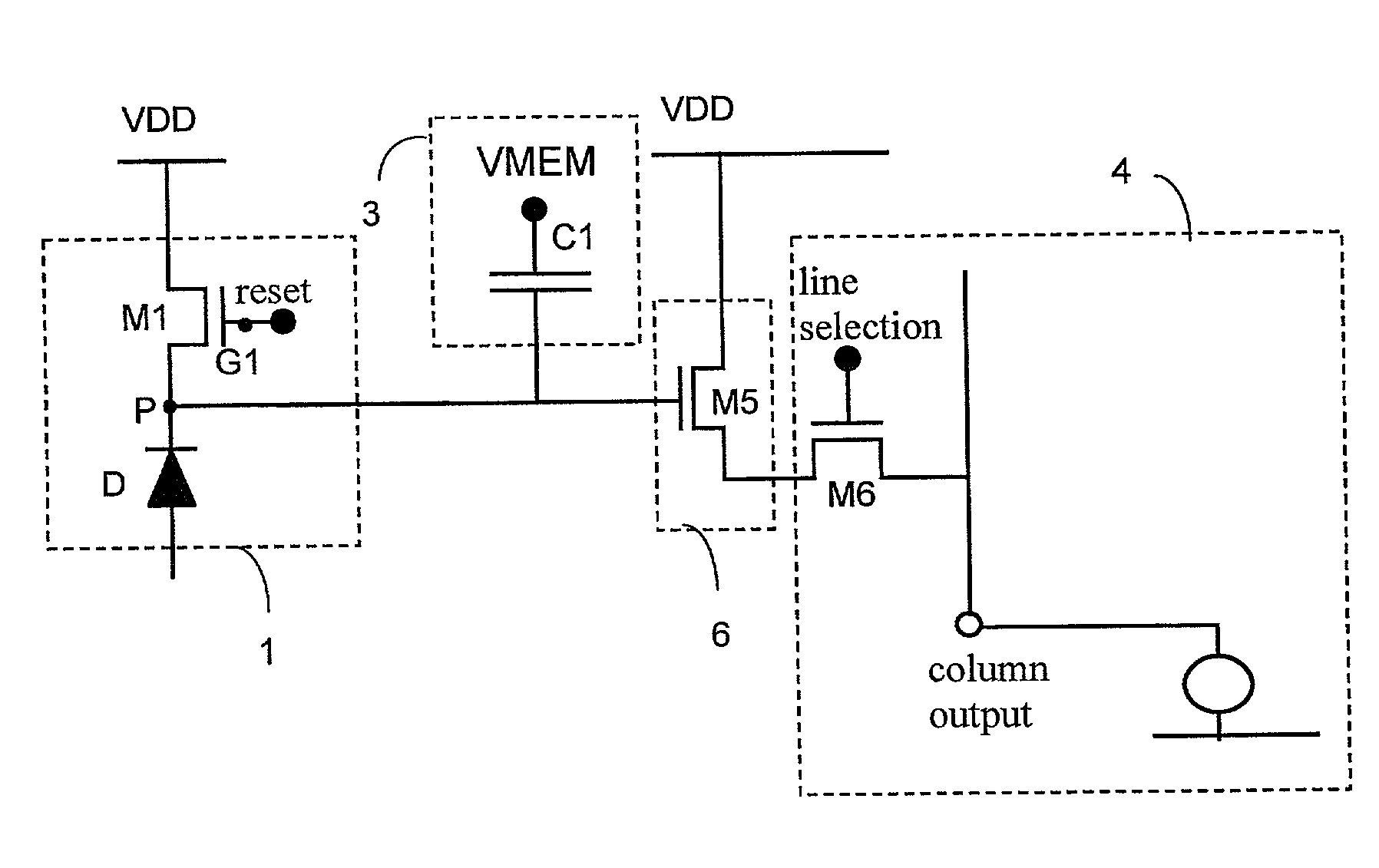
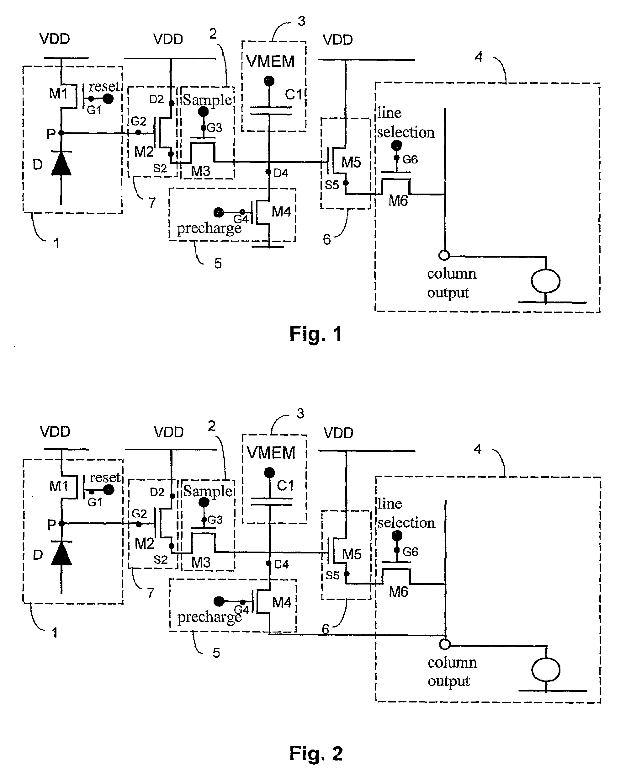
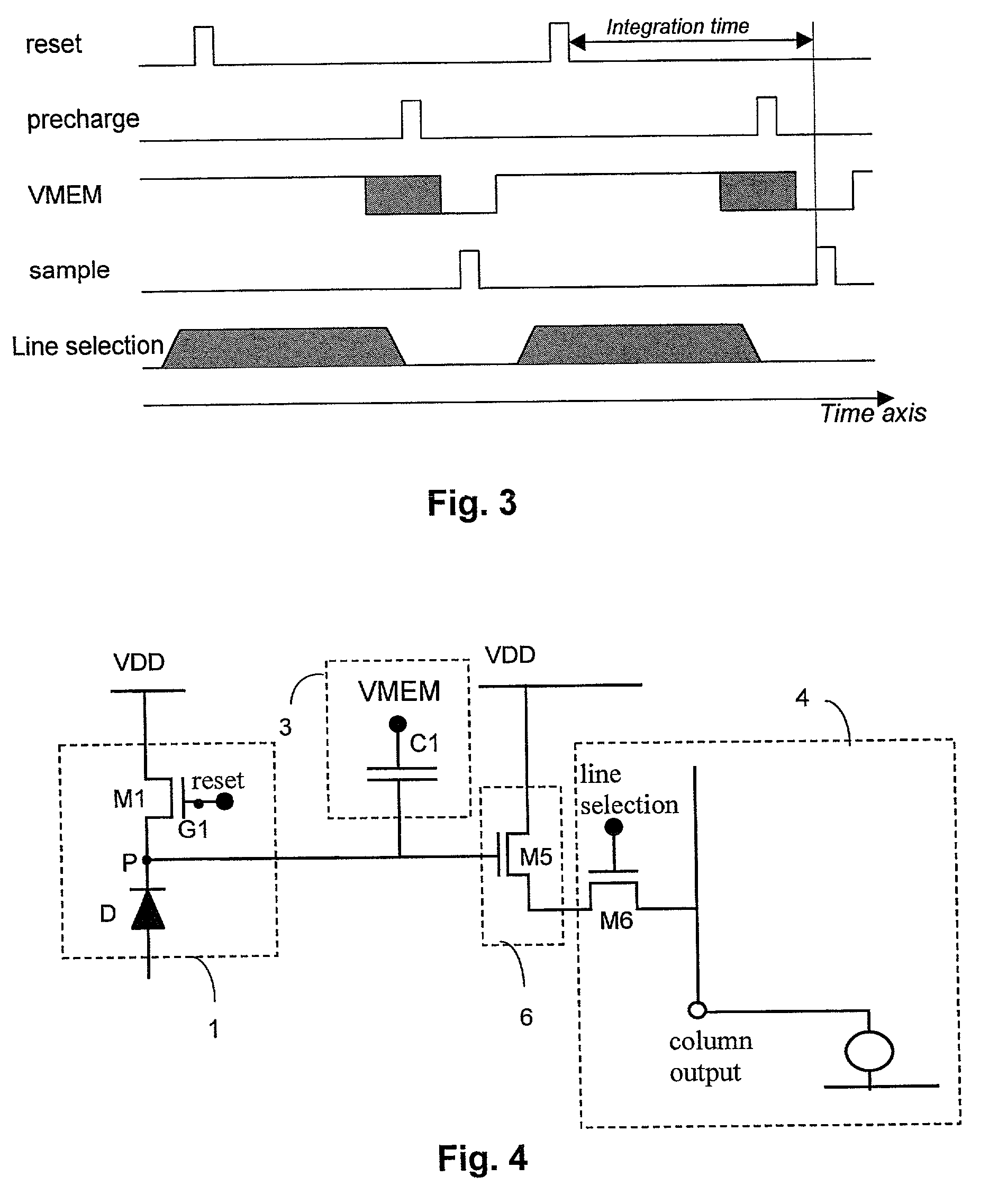
[0034]FIGS. 1 and 4 principally depict in schematic form an active pixel according to the present invention, FIG. 4 illustrating the most simple embodiment, and FIG. 1 illustrating a more elaborate embodiment.

[0035]The input signal to an active pixel is the radiation intensity at the location of that pixel. The radiation may be any of optical light, IR light, UV light, high energy particles, X-rays, etc. In the following the embodiments of the present invention will be described with reference to incident light. The incident light intensity is transduced by a photodiode (the senso...


PUM


Abstract

An active pixel comprises a sensor circuit for collecting radiation induced charges and transducing them to a measurement signal corresponding to the amount of charge collected, and a capacitor element with two nodes, where the measurement signal is present on a node of the capacitor element. The memory circuit is clocked, i.e. driven by a pulsed signal. The pulse on the memory circuit will rise the reset level at the output, which is lowered due to threshold voltage losses in the active pixel circuit, thus restoring a large signal swing. Arrays of the pixels are described, as well as a method for reading out such a pixel.

Description

TECHNICAL FIELD OF THE INVENTION[0001]The present invention relates to a method for adjusting the signal level of an active pixel, and an active pixel wherein the signal level can be adjusted.[0002]Such an active pixel can be used e.g. as an active pixel for synchronous detection. With synchronous detection is meant a technique for sensing the time variation of collected photocharges with synchronous excitation of a sensor element and detection of the photocharges collected thereon.BACKGROUND OF THE INVENTION[0003]From Orly Yadid-Pecht & al., “A random access photodiode array for intelligent image capture”, IEEE transactions on electron devices, vol. 38, no. 8, p.1772 (August, 1991) is known a sensor comprising a light detection unit, an information sampling and holding unit, and a reading unit. The light detection unit comprises a reverse-biased photodiode coupled in series with a reset transistor, which is coupled to a positive power supply. The connection point between the photod...

Claims


Application Information

Patent Timeline
IPC IPC(8): H04N5/335H04N5/363H04N5/3745
CPCH04N5/37452H04N25/771
Inventor DIERICKX, BART
Owner SEMICON COMPONENTS IND LLC
Learn More