Method of inspecting a DNA chip

Inactive Publication Date: 2007-05-15
HITACHI LTD
View PDF10 Cites 54 Cited by
  • Summary
  • Abstract
  • Description
  • Claims
  • Application Information

AI Technical Summary

Benefits of technology

[0012]The inspection of a DNA chip to be inspected is executed in the following steps: Irradiating mutually different positions with a plurality of M excitation lights simultaneously with the use of an objective lens for a time Δt that is longer than a fluorescent light attenuation time, the excitation lights including a spot diameter d that is smaller than a dimension D of each cell, guiding obtained fluorescent lights to a fluorescent light detecting optical path, detecting the fluorescent lights on an image-forming plane that is in a conjugation relationship with irradiation spots onto the DNA chip, and executing the inspection of the DNA chip from positions and intensities of the fluorescent lights. At this time, the spot diameter is set to be substantially 1 / N of an integer N indicating the cell dimension. Moreover, relative positions between the irradiation spots and the DNA chip are caused to differ j times in sequence so as to inspect the entire inspection target positions LN2=Mj. Here, L denotes the cell number within the chip. Also, N is made equal to 2 or more and each cell is divided into a plurality of portions so as to select and process only significant data out of N2 data existing within one call, thereby executing the precise inspection. Executing the inspection in this way allows the fluorescent lights to be detected in a time less than LN2 / (6×10⁵) sec with reference to the entire inspection target sample-point number LN2 of the DNA chip.
[0081]Also, the present invention is not only applied to the DNA inspection, but is widely used for a fluorescent light detecting microscopic method. The present invention tremendously shortens the times that have been required for the conventional observations and inspections. Namely, it becomes possible to detect, in a short time, even a weak light toward which only several photons can be detected. Also, it becomes possible to execute, in a short time and with a high-accuracy, the detection over a broad range ranging from the weak light to the strong light to be detected.

Problems solved by technology

In the conventional technologies, however, it takes so much inspection time to irradiate one point with the excitation light spot, which is equivalent to a necessary inspecting resolution of the DNA chip, and to detect the obtained fluorescent lights one after another.
Transferring the detection to the next detection point without waiting for the finishing of the fluorescent light generation makes the detection itself impossible.
However, all of the generated fluorescent lights are not detected.
As a result, half or more of the laser beam energy emitted from the laser light-source turns out to be wasted.
In the above-described apparatus, however, no sufficient consideration has been given to this point.
Moreover, making the spot diameter smaller lessens the number of the fluorescent molecules existing within the spot diameter, thereby lowering the detection sensitivity.
Increasing the scanning rate, however, shortens the excitation time for the fluorescent material, thereby lessening the fluorescence intensity or increasing a circuit noise to lower the detection sensitivity.
Namely, implementing the high-resolution characteristic, implementing the high-speed characteristic and implementing the high-sensitivity characteristic are contradicted to each other, and accordingly it was difficult to accomplish them.
Accordingly, it is difficult to equate all the light intensities of the plurality of irradiation spots.
In this case, however, the light utilization efficiency is no good and the light intensities are decreased, thus resulting in such a problem that the detection sensitivity is deteriorated.
As a result, when the fluorescent light is extremely weak, it takes a time to execute the detection equivalent to the one-pixel.
Consequently, it takes a considerable amount of time to detect the entire 2-dimensional image.
Executing the detection in such a short time makes it difficult to detect the fluorescent light detection intensity in a broad dynamic range (for example, 216).
This condition requires a considerable amount of time to be spent to detect the weak fluorescent light.

Method used


Image

  • Method of inspecting a DNA chip
  • Method of inspecting a DNA chip
  • Method of inspecting a DNA chip

Examples


Embodiment Construction

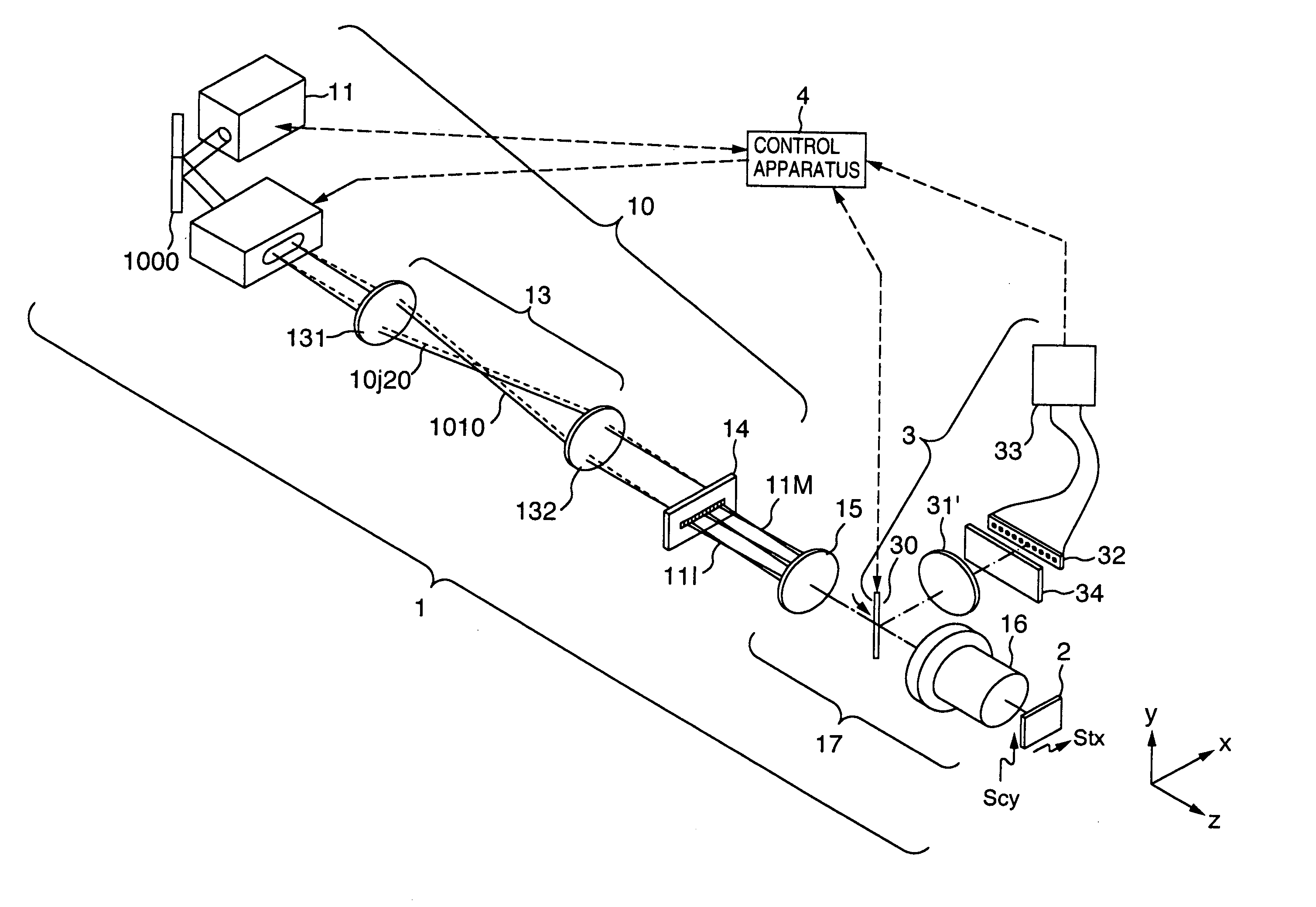
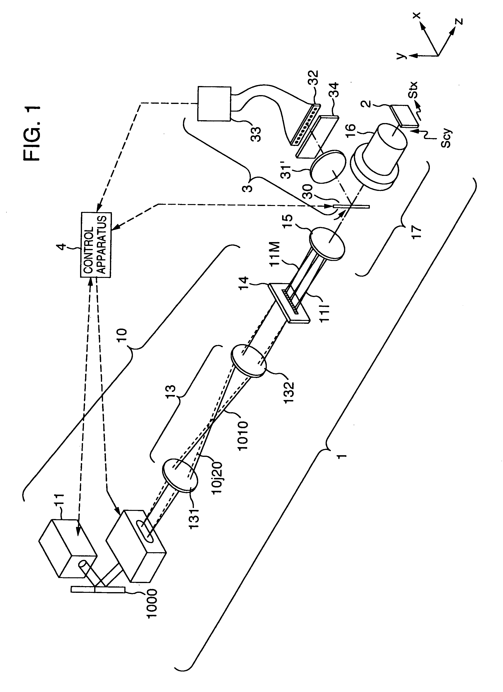
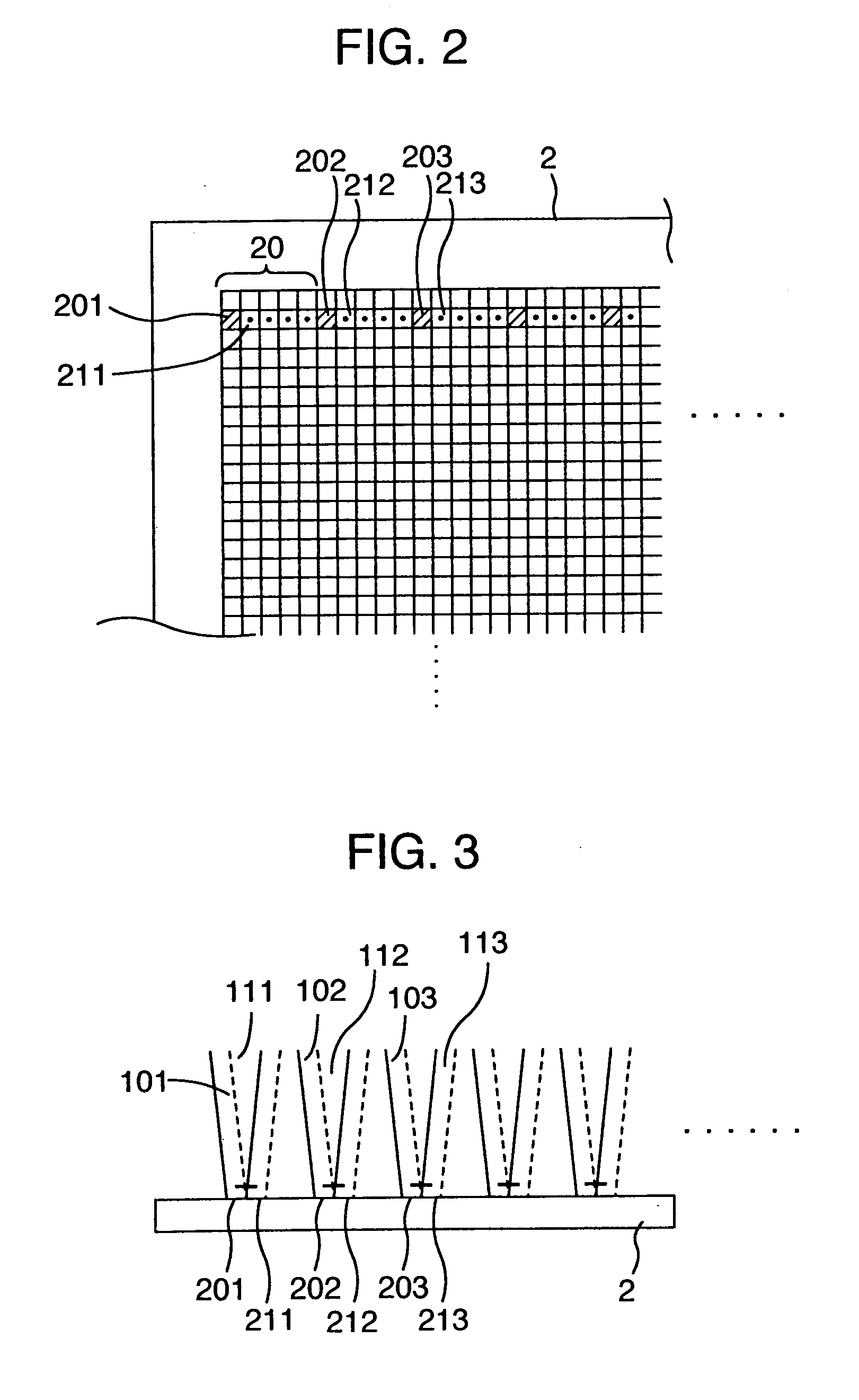
[0163]FIG. 1 is a diagram for illustrating an embodiment in the present invention. The reference numerals denote the following configuration components: 1 A multi-spot excitation lights-irradiating system for forming multi-spot excitation lights to irradiate a DNA chip 2 with the excitation lights so that a fluorescent light detection can be executed, 3 a fluorescent light detecting system for detecting fluorescent lights generated by the multi-spot excitation lights, 11 an excitation light-source including an excitation light light-source and an excitation light beam forming optical system. A He—Ne laser light beam is formed into a desired longitudinal-to-transverse ratio of the beam diameter by two cylindrical lenses having different focal lengths, then being launched into an AO deflector 12 through a mirror 1000. The AO deflector 12 includes a terminal of a frequency-ωhigh-frequency voltage applied to a quartz oscillator, and an input terminal of an amplitude signal the frequency...


PUM

PropertyMeasurementUnit
Lengthaaaaaaaaaa
Lengthaaaaaaaaaa
Timeaaaaaaaaaa

Abstract

A method of inspecting a DNA chip and an apparatus therefor that allow a picture to be reconstructed in the following steps: A plurality of irradiation spots are formed on a DNA probe array mounted on a stage. Then, the stage is displaced in X, Y directions so as to execute a scanning, thereby irradiating substantially all the entire surface of the DNA probe array. Next, a plurality of emitted fluorescent lights, which are generated from the plurality of irradiation spot portions on the DNA probe array, are converged and are then detected simultaneously by multi detectors. Finally, a data processing apparatus processes the detected signals, thereby reconstructing the picture.

Description

BACKGROUND OF THE INVENTION[0001]The present invention relates to an apparatus for reading and analyzing an emitted light (fluorescent light) pattern emitted from a sample located on a plane. More particularly, it relates to a method and an apparatus by which living body samples, such as a DNA, a RNA and an oligonucleotide marked by a fluorescent material, are trapped at a plurality of positions on a substrate so as to read an emitted light pattern from the fluorescent marker with a high-resolution, at a high-speed and with a high-sensitivity.[0002]Analysis technologies for analyzing the DNA and proteins are important in fields of medicine and biology including gene analysis and gene diagnosis. In particular, in recent years, attention has been focused on a method and an apparatus by which, using a DNA probe array (which is called in other way by various names such as oligochip, DNA chip or biochip, but hereinafter the DNA probe array is employed as the generic name), a variety type...

Claims


Application Information

Patent Timeline
IPC IPC(8): G01N33/00C07H21/04C12M3/00C12Q1/68G01N33/53H01J3/14
CPCG01N21/6428G01N21/6452G01N21/6456Y10T436/143333Y10S436/80
Inventor OSHIDA, YOSHITADANAKATA, TOSHIHIKOSAKATA, TOMOAKIYASUDA, KENJITAKAHASHI, SATOSHI
Owner HITACHI LTD
Why Eureka
Try Eureka