Method for manufacturing semiconductor device

Inactive Publication Date: 2007-04-03
SK HYNIX INC +1
View PDF16 Cites 1 Cited by
  • Summary
  • Abstract
  • Description
  • Claims
  • Application Information

AI Technical Summary

Benefits of technology

[0009]Further, the present invention can be used to prevent the damage of a tunnel oxide film caused by penetration of a chemical solution used in the manufacturing process of a flash device.
[0010]According to a preferred embodiment of the present invention, there is provided a method for preventing a deterioration of a property in the semiconductor device, wherein the deterioration results from damage of the lower layer generated by penetration of a chemical solution used in the manufacturing process of a flash device.
[0011]According to another embodiment of the present invention, a method is provided for manufacturing a semiconductor device comprising the steps of; providing a semiconductor substrate having a lower layer; and forming at least 2-layered film to prevent a solution used in the subsequent processes from penetrating the lower layer, and subjecting N2 purge process to an upper face in the lower film of said 2-layered film, to have a different grain boundary structure at border of the films, whereby changing the grain boundary structure of the upper face in the lower film.

Problems solved by technology

However, since the solution is capable of penetrating a lower layer there below, it may damage the lower layer when used.
The tunnel oxide film and the semiconductor substrate are damaged due to penetration of the chemical solution.
As a result, the tunnel oxide film is damaged when a program operation and an erase operation are performed in the flash device by fouler nordheim (F-N) Tunneling method, so that the leakage current from a channel or a contact layer to a floating gate is subject to generate, resulting in the characteristic of the flash device deteriorating.

Method used


Image

  • Method for manufacturing semiconductor device
  • Method for manufacturing semiconductor device
  • Method for manufacturing semiconductor device

Examples


Embodiment Construction

[0019]The above and other objects, features and advantages of the present invention will become apparent from the following descriptions and the appended claims, taken in conjunction with the accompanying drawings in which like parts or elements denoted by like reference symbols.

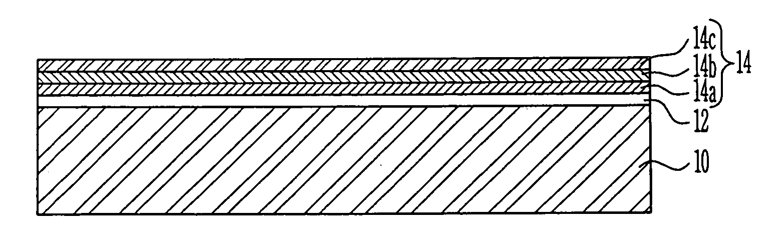
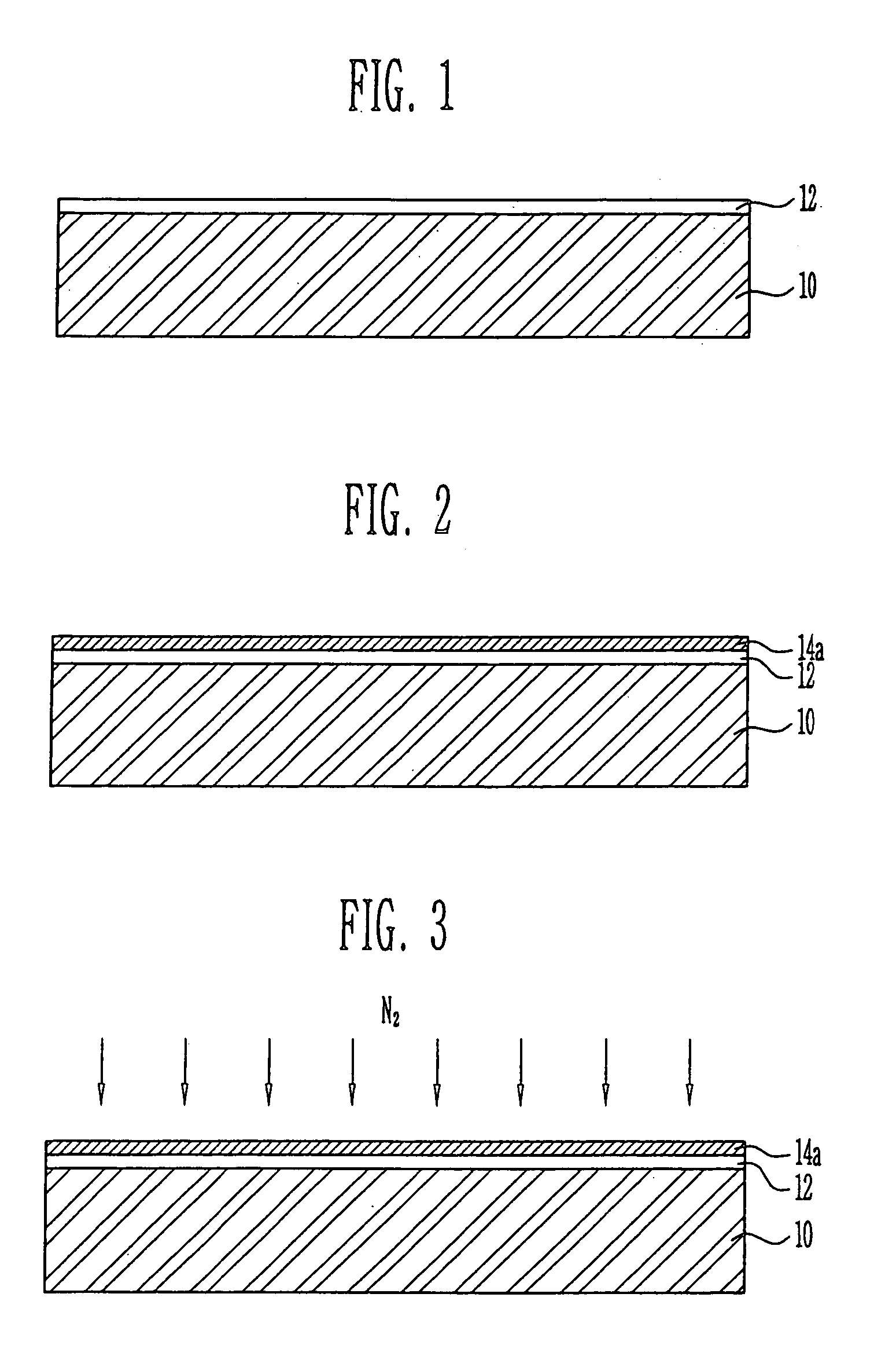
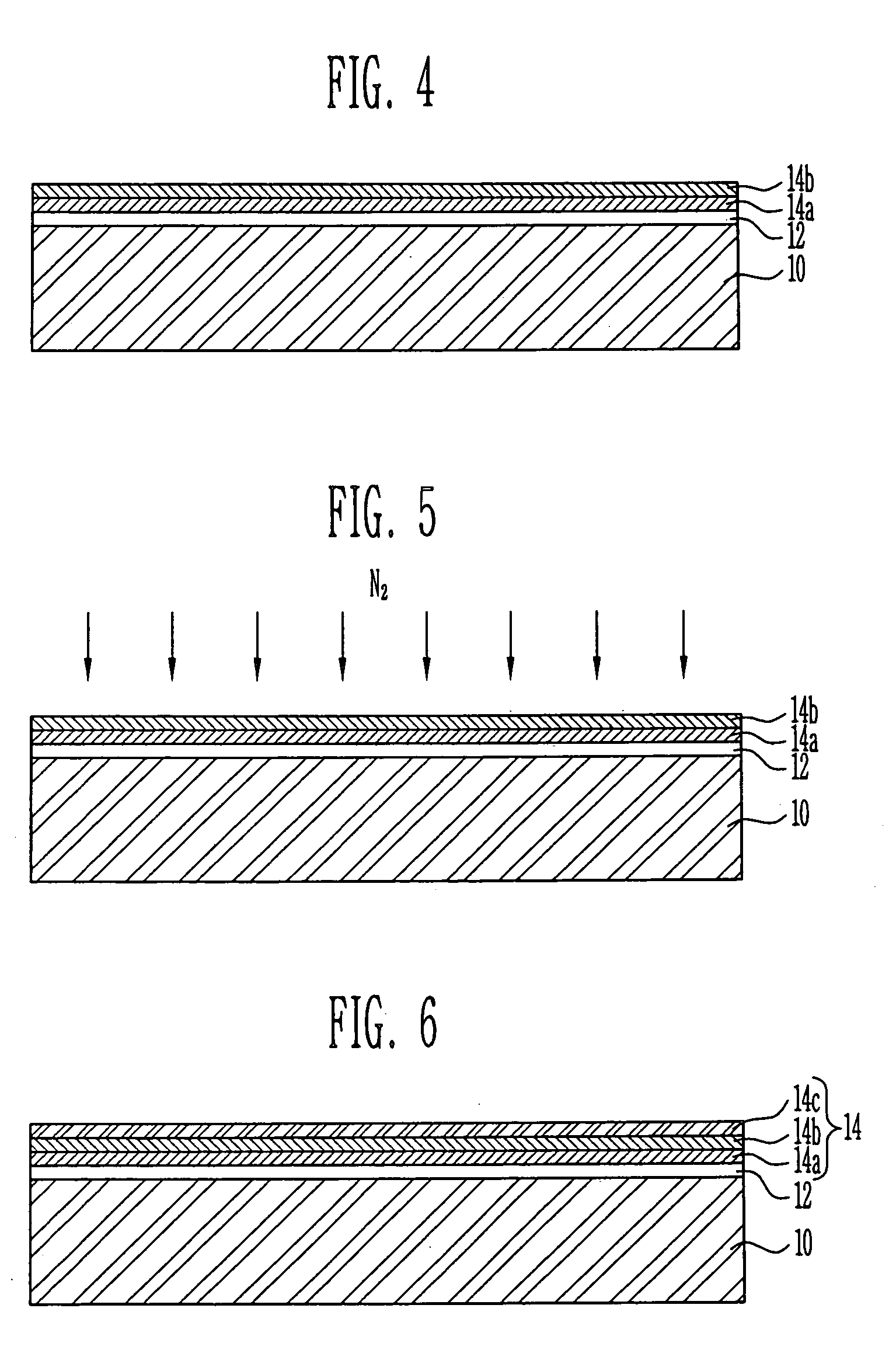
[0020]FIGS. 1 to 6 are cross-sectional views for explaining a method for manufacturing a semiconductor device according to a preferred embodiment of the present invention sequentially. Table.1 shows process recipes used in the process of FIGS. 1 to 6

[0021]

TABLE 1gasPressureTemperaturestepTime(min)SiH4N2(Torr)(° C.)The firstpre-deposition1125 ccNot use0.2620processstepDepositionX(variable)250 ccNot use0.2620stepPumping step1ClosedNot useNot620(excluding)appliedPurgeN2 purge step1Not useOpened0.2620processThePre-deposition1OpenedClosed0.2620secondstep(supplying)processDepositionXOpenedNot use0.2620stepPumping step1ClosedNot useNot620appliedPurgeN2 purge step1Not useOpened0.2620processThe 3rdPre-deposition1Open...


PUM


Abstract

Provided is a method for manufacturing a semiconductor device capable of preventing a solution from penetrating a lower layer by forming a poly silicon layer stacked of the films having the different grain boundary structures at border, wherein the solution is used in the subsequent strip and cleaning process.

Description

BACKGROUND[0001]1. Field of the Invention[0002]The present invention relates to a method for manufacturing a semiconductor device and, more particularly, to a method for manufacturing a semiconductor device capable of preventing a chemical solution from penetrating a lower layer, wherein the chemical solution is used at the time of performing a strip process and a cleaning process in the manufacturing process of the semiconductor device.[0003]2. Discussion of Related Art[0004]Conventionally, a strip process and a cleaning process are performed in a manufacturing process of a semiconductor device. In the strip process and the cleaning process, a chemical solution such as HF and buffered oxide etchant (BOE; the mixed solution of HF and NH4F as 100:1 or 300:1) etc., is used. However, since the solution is capable of penetrating a lower layer there below, it may damage the lower layer when used.[0005]For example, in the manufacturing process of a flash device, shallow trench isolation (...

Claims


Application Information

Patent Timeline
IPC IPC(8): H01L21/20H01L21/28H01L21/8247H01L21/30H01L21/304H01L21/321H01L27/115H01L29/788H01L29/792
CPCH01L21/3211H01L21/28273H01L29/40114H01L21/304
Inventor LEE, CHANG JIN
Owner SK HYNIX INC
Why Eureka
Try Eureka