
Method of interfacing ancillary equipment to FIMS processing stations

a technology of ancillary equipment and processing stations, which is applied in the direction of individual semiconductor device testing, semiconductor/solid-state device testing/measurement, instruments, etc., can solve the problems of slow manufacturing process, inability to easily translate processing corrections from measurement and inspection systems to fims stations, and down time between fims stations and measurement and inspection systems

Active Publication Date: 2007-03-06
KLA TENCOR TECH CORP
View PDF9 Cites 14 Cited by
  • Summary
  • Abstract
  • Description
  • Claims
  • Application Information

AI Technical Summary

Benefits of technology

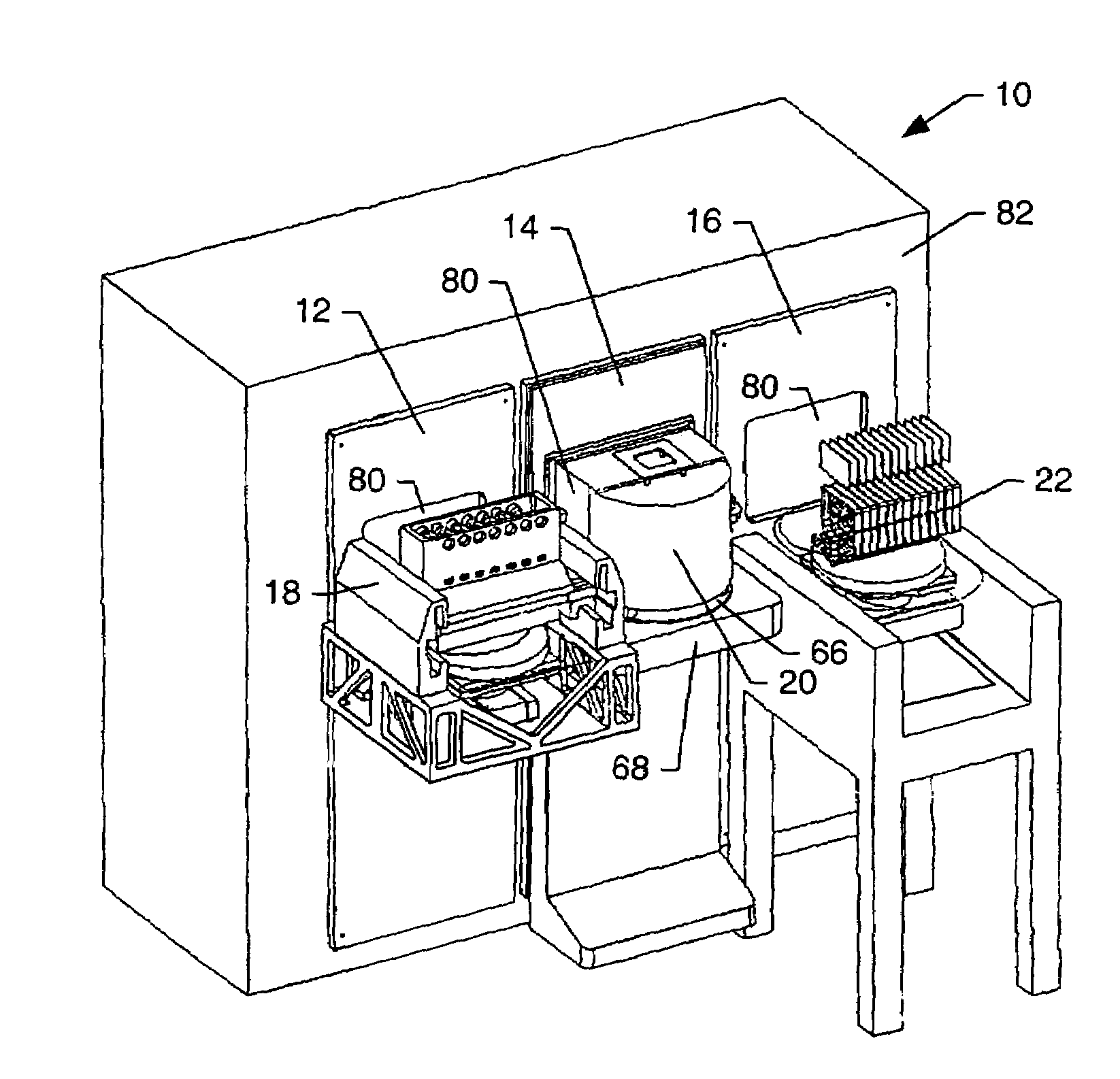
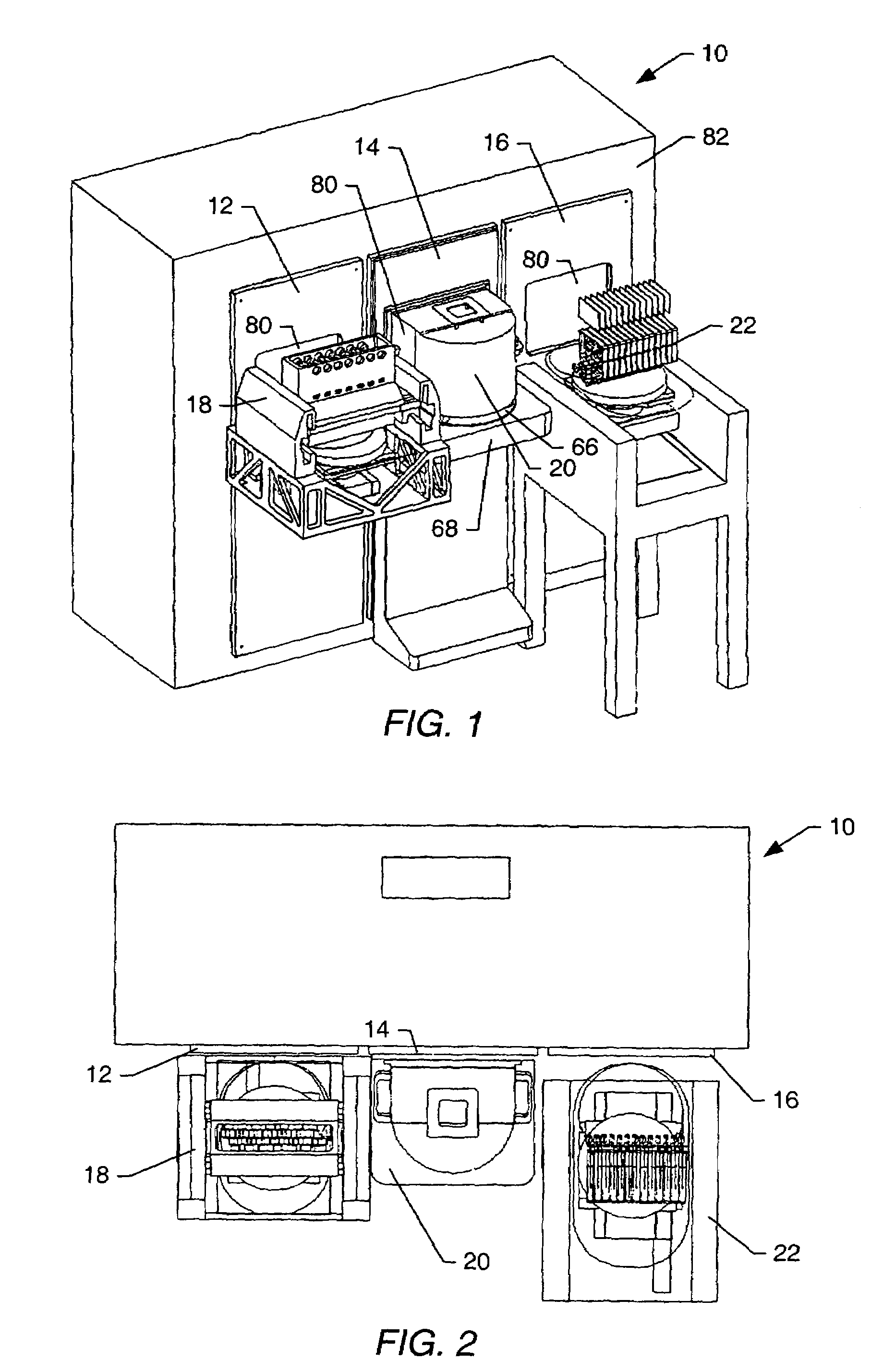
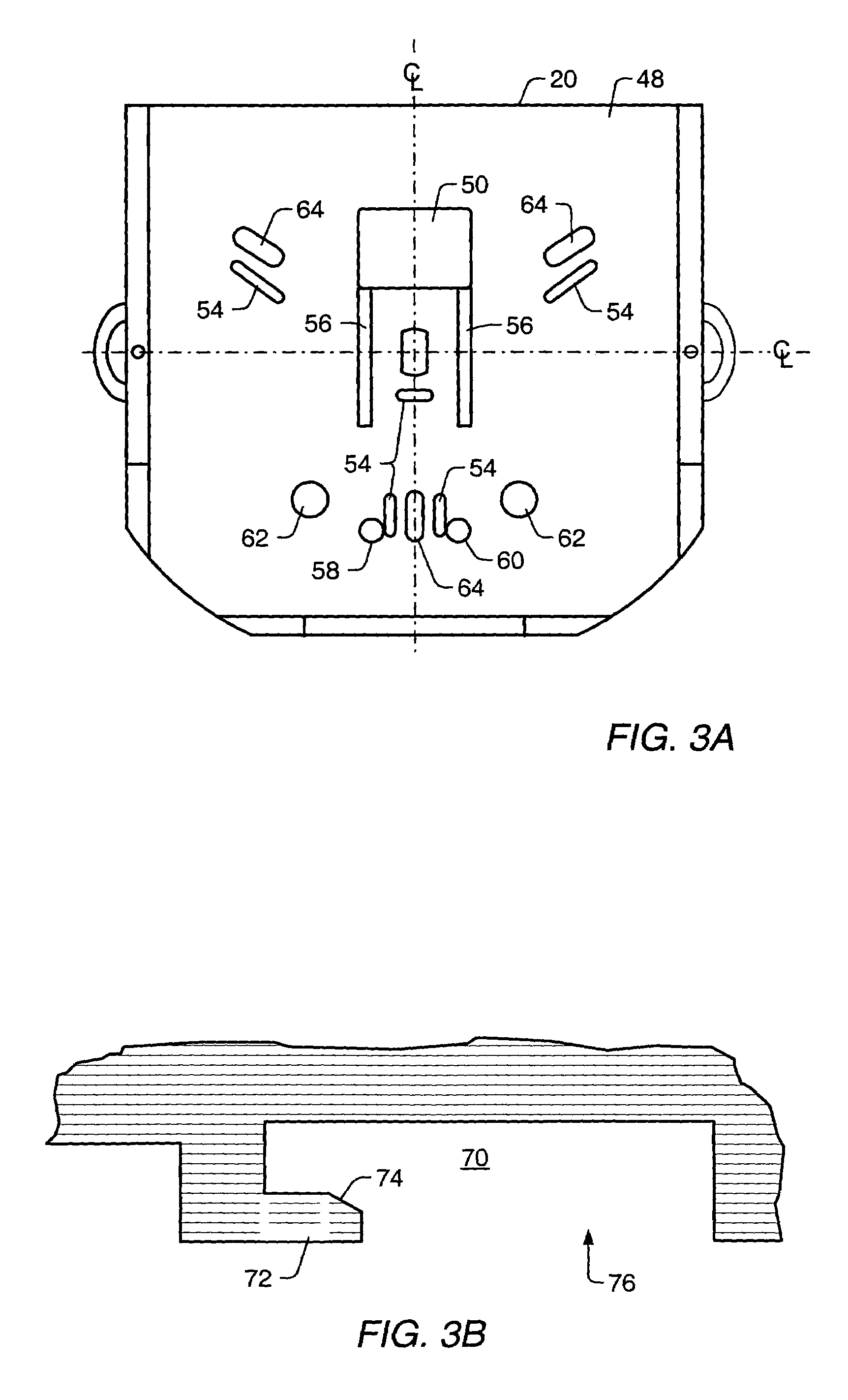
[0010]Preferred ancillary equipment includes a process diagnostic tool that is integrated into an independent automated semiconductor specimen fabrication station to make it more efficient and flexible to use. The process diagnostic tool performs on the semiconductor specimen a processing operation that otherwise would not be performed by fabrication station processing components. The process diagnostic tool preferably is a module (hereafter “PDM”) that performs, for example, a measurement or an inspection function. The PDM is built to fit within the allowable envelope specified by the industry guidelines and standards and to mount to any load port of a FIMS station. The PDM is matable to a FIMS station in the same sense as a FIMS-compatible wafer cassette transport box is matable to a FIMS box door at a FIMS load port interface aperture.

Problems solved by technology

This procedure results in logistical problems and interruptions that slow the manufacturing process.
Accordingly, processing corrections cannot be easily translated from the measurement and inspection systems to the FIMS station.
Moreover, the amount of time an operator spends moving a wafer cassette transport box to and from the FIMS station results in down time in the FIMS station and the measurement and inspection system.

Method used


Image

  • Method of interfacing ancillary equipment to FIMS processing stations
  • Method of interfacing ancillary equipment to FIMS processing stations
  • Method of interfacing ancillary equipment to FIMS processing stations

Examples


Embodiment Construction

[0020]This invention entails integrating a measurement or an inspection system in the form of a PDM onto or into an independent, automated manufacturing system of semiconductor wafers. The latter of such systems includes a semiconductor process tool and is preferably a FIMS station. Processes carried out by a PDM could be but are not limited to defect inspection, particle inspection, film thickness measurement, circuit pattern overlay fidelity measurement, or circuit critical dimension (CD) measurement. An example of an inspection system that can be configured in the form of a PDM is described in U.S. patent application Ser. No. 09 / 070,437, filed Apr. 30, 1998, for A System and Method for Inspecting Semiconductor Wafers, which issued as U.S. Pat. No. 6,020,957 to Rosengaus et al. and which is assigned to the assignee of the present patent application and is incorporated by reference herein.

[0021]The invention provides added capability to the FIMS station onto or into which a PDM is ...


PUM


Abstract

This invention includes a method of integrating into a semiconductor specimen fabrication station a process diagnostic module that performs on the semiconductor specimen a processing operation that otherwise would not be performed by the processing components to thereby make the fabrication station more efficient and flexible to use. The process diagnostic module includes, for example, a specimen parameter measurement system or a specimen inspection system and is configured to mount on a front-opening interface mechanical standard (FIMS) load port and fits within the allowable spatial envelope. This invention further includes located external to the semiconductor specimen fabrication station a processor that receives and processes data acquired by the process diagnostic module during its operation.

Description

PRIORITY CLAIM[0001]This application claims priority to U.S. Provisional Application No. 60 / 226,336 filed Aug. 18, 2000.TECHNICAL FIELD[0002]This invention relates to front-opening interface mechanical standard (FIMS) semiconductor device processing stations and, in particular, to a method of interfacing ancillary equipment to FIMS stations to make better, more flexible use of them.BACKGROUND OF THE INVENTION[0003]The fabrication of semiconductor devices entails numerous processing operations such as parameter measurements and inspections of semiconductor wafers on which the devices are formed during various stages of their development. Current semiconductor wafer inspection and measurement systems are separate stand-alone machines to and from which an attendant often manually transports the semiconductor wafers in a clean room environment. This procedure results in logistical problems and interruptions that slow the manufacturing process.[0004]Semiconductor wafer processing is also...

Claims


Application Information

Patent Timeline
Patent Type & Authority Patents(United States)
IPC IPC(8): G06F19/00
CPCH01L21/67775
Inventor ASHKENAZ, SCOTTLARSON, C. THOMAS
Owner KLA TENCOR TECH CORP
Learn More