Organic electro-luminescent display device and method for manufacturing the same
- Summary
- Abstract
- Description
- Claims
- Application Information
AI Technical Summary
Benefits of technology
Problems solved by technology
Method used
Image
Examples
example 1
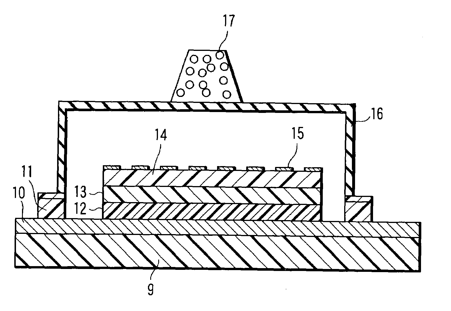
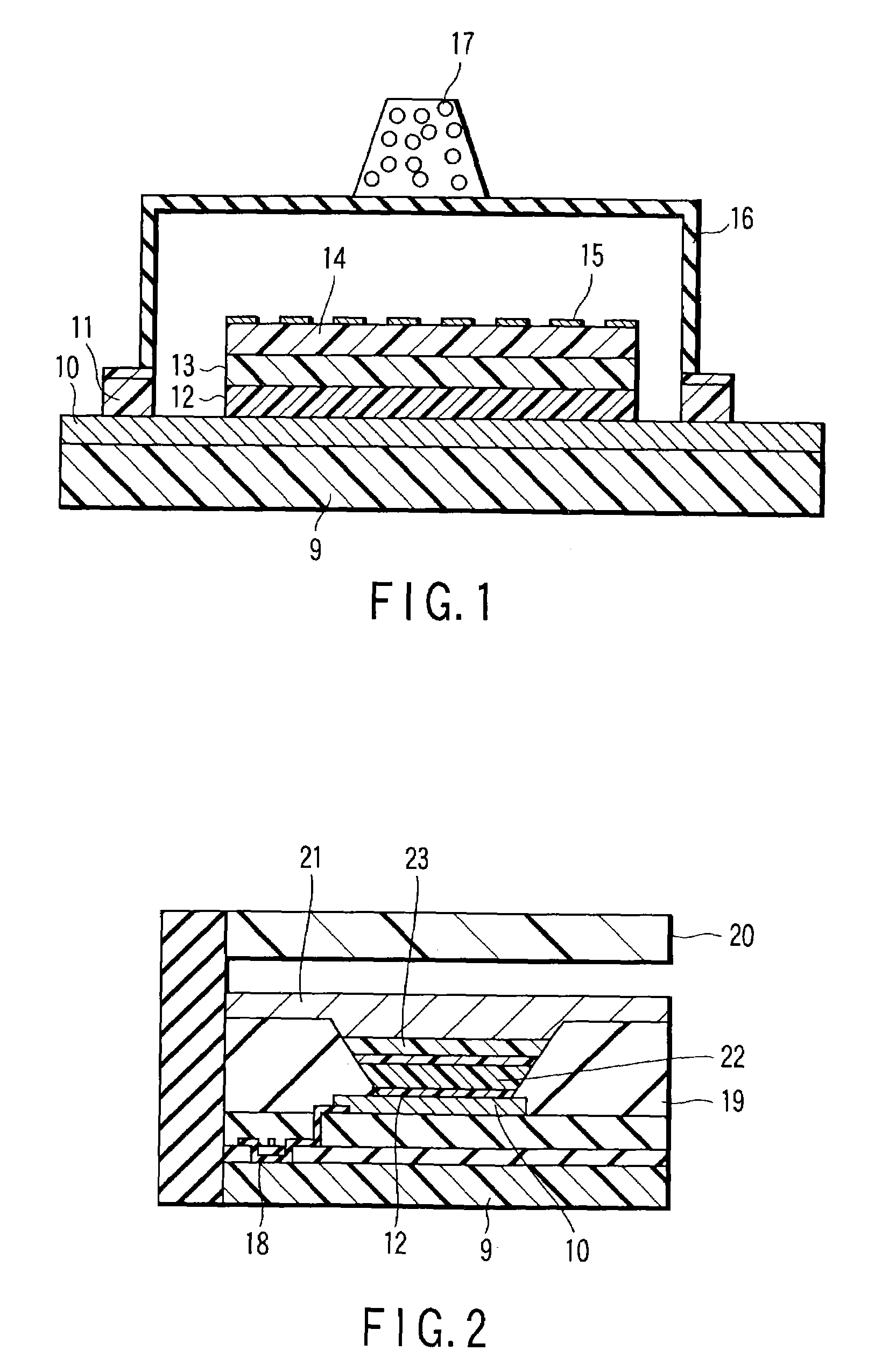
[0133]A material represented by the aforementioned chemical formula (8) for forming a hole transferring layer was vapor-deposited on the surface of an ITO-attached substrate to form the hole transferring layer, thus preparing a low molecular type organic EL display device having a structure as shown in FIG. 1. More specifically, an ITO (indium-tin-oxide) film having a thickness of 100 nm was formed as a transparent electrode (anode) 10 on the surface of a glass substrate 9. Then, a compound represented by the aforementioned chemical formula (8) was vapor-deposited on the transparent electrode 10 to form a hole transferring layer 12 having a thickness of 60 nm.
[0134]Alq3 (tris(8-quinolilato)aluminum) was employed as a material for the light emitting layer 13 and vapor-deposited on the hole transferring layer 12 to form the light emitting layer 13. An MgF2 buffer layer having a thickness of about 10 nm was deposited over the light emitting layer 13, and then, an Al film having a thick...
example 2
[0137]The same procedures as explained in Example 1 were repeated except that as a material for the hole transferring layer, a compound represented by the aforementioned chemical formula (9) was substituted for the compound employed in Example 1 as a material for the hole transferring layer, thereby manufacturing a low molecular type organic EL display device as shown in FIG. 1.
[0138]The EL display device thus obtained was subjected to a continuously actuation for ten thousand hours in the same manner as conducted in Example 1. As a result, the luminance thereof after this experiment was found 80% relative to the initial value of luminance, and any pixel which ceased to emit any longer was not recognized at all.
example 3
[0139]The same procedures as explained in Example 1 were repeated except that as a material for the hole transferring layer, a compound represented by the aforementioned chemical formula (10) was substituted for the compound employed in Example 1 as a material for the hole transferring layer, thereby manufacturing a low molecular type organic EL display device as shown in FIG. 1.
[0140]The EL display device thus obtained was subjected to a continuously actuation for ten thousand hours in the same manner as conducted in Example 1. As a result, the deterioration in luminance thereof was confined within 20%, and any pixel which ceased to emit any longer was not recognized at all. Since the compound employed in this example was especially large in asymmetry of the molecular structure thereof, it was considered possible to prevent the generation of defects such as partial crystallization.
PUM
| Property | Measurement | Unit |
|---|---|---|
| Transparency | aaaaa | aaaaa |
| Phosphorescence quantum yield | aaaaa | aaaaa |
Abstract
Description
Claims
Application Information
 - R&D
- Intellectual Property
- Life Sciences
- Materials
- Tech Scout
- Unparalleled Data Quality
- Higher Quality Content
- 60% Fewer Hallucinations
Browse by: Latest US Patents, China's latest patents, Technical Efficacy Thesaurus, Application Domain, Technology Topic, Popular Technical Reports.
© 2025 PatSnap. All rights reserved.Legal|Privacy policy|Modern Slavery Act Transparency Statement|Sitemap|About US| Contact US: help@patsnap.com


