
Addressing process and device for a bistable liquid crystal screen

a liquid crystal display and bistable technology, applied in the direction of optics, instruments, non-linear optics, etc., can solve the problems of affecting the electro-optical response of the liquid crystal pixel, affecting the addressing process, and affecting the addressing time, so as to reduce the parasitic optical effect of addressing and reduce the time c

Inactive Publication Date: 2007-02-06
NEMOPTIC
View PDF7 Cites 5 Cited by
  • Summary
  • Abstract
  • Description
  • Claims
  • Application Information

AI Technical Summary

Benefits of technology

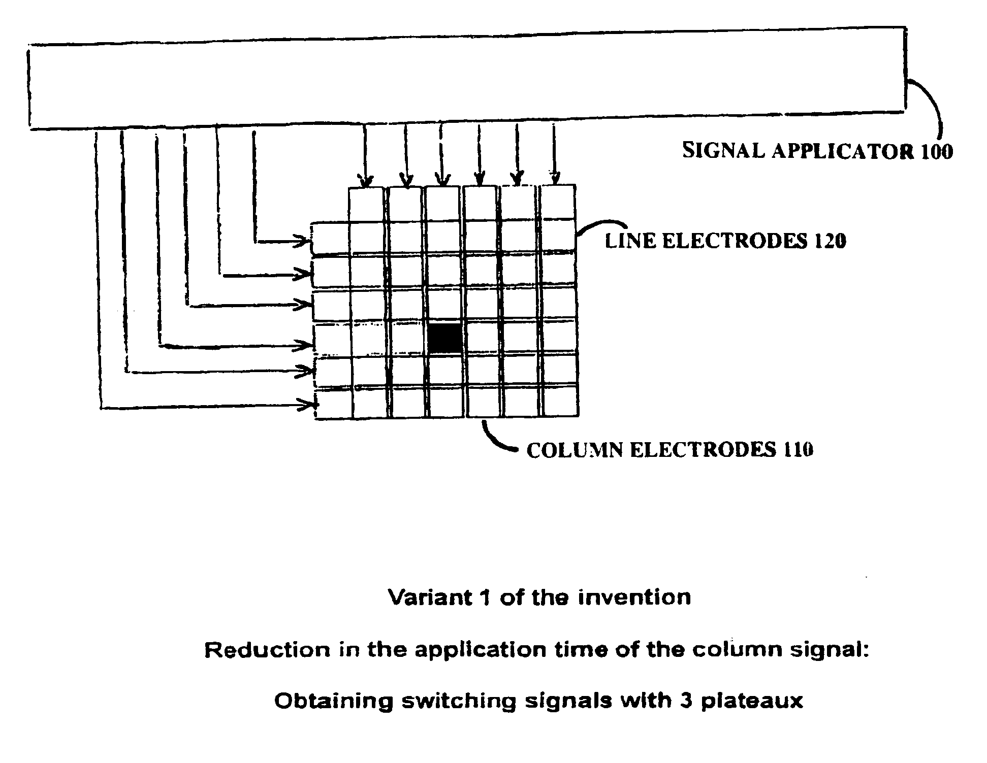
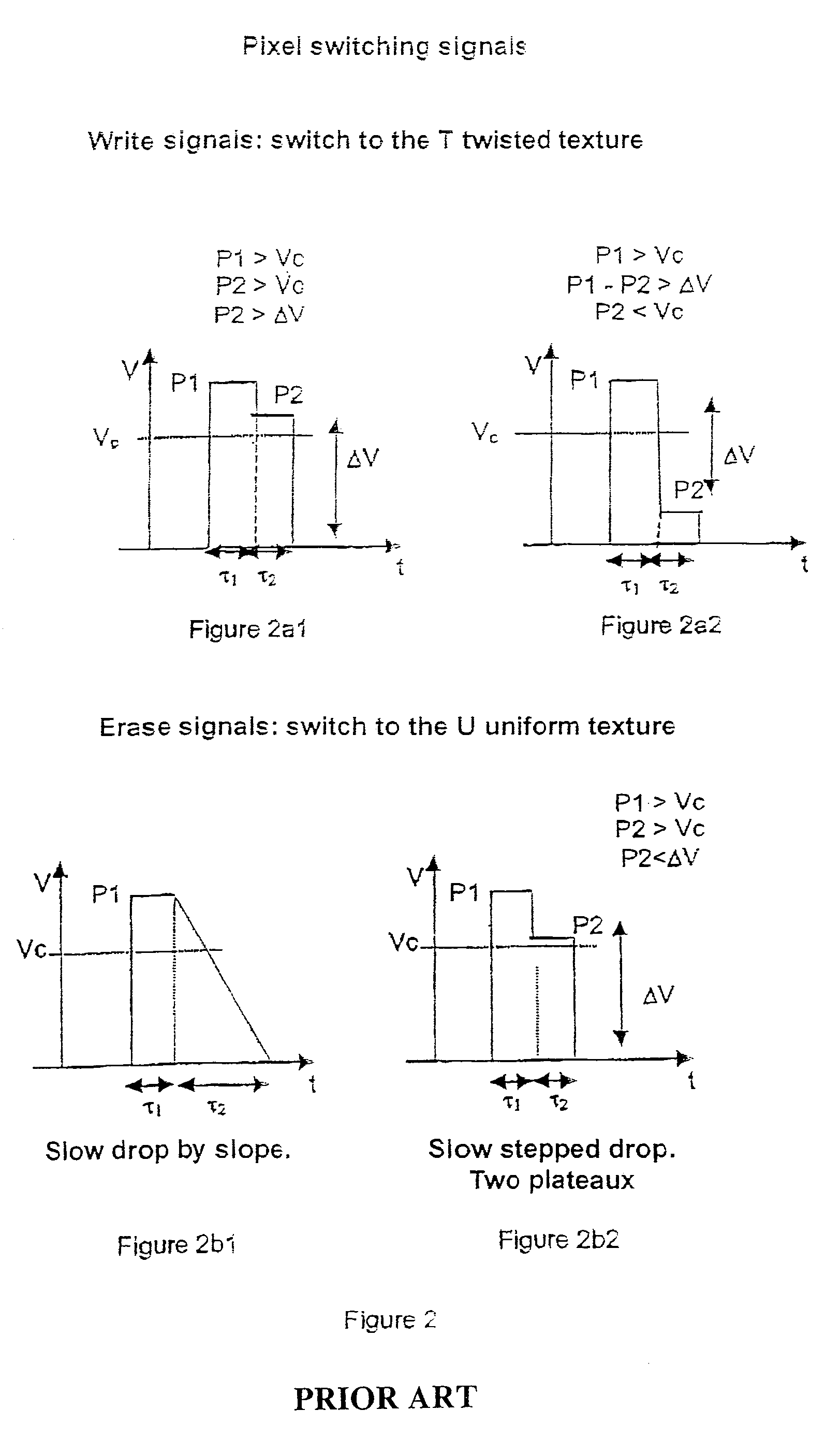
"The patent proposes a new process to eliminate the dither effect in a liquid crystal screen. This involves modifying the column signal to reduce the Vrms value and synchronize its drop with the line pulse. The process includes applying an electrical signal to the screen column with parameters that reduce the mean quadratic voltage of the parasite pixel pulses. Two variants are proposed to achieve this result: reducing the time during which the column signal is applied and changing the form of the column signal to reduce the effective voltage. The invention also proposes a dot matrix screen addressing device."

Problems solved by technology

The drawback with passive multiplexing is that a pixel is sensitive to the column signals throughout the time that the image is addressed, and not just when its line is activated.
We can consider that the signals applied to the pixel outside of the time its line is selected as parasite signals, which interfere in the electro-optical response of the liquid crystal pixel.
Nevertheless, they cause temporary disruptions to the optical response by deforming the texture of the pixel without breaking either the strong or weak anchoring.
The optical appearance may be severely disrupted during the total duration of the addressing of the screen.
This may cause for example dither, a loss of image contrast, etc.
If the total time required to address the image is short, the dither of the image is not easy to see by the observer.
Too low of a value for C will not allow the change to be made between two textures.
This method unfortunately increases the image write time,.
Furthermore, if the inequality (3) is not respected, this option is not effective.

Method used


Image

  • Addressing process and device for a bistable liquid crystal screen
  • Addressing process and device for a bistable liquid crystal screen
  • Addressing process and device for a bistable liquid crystal screen

Examples


example 1

[0105]By way of a first example, we will take a sloped type column signal. The amplitude of this signal increases linearly with time until it reaches a maximum peak voltage C″, then is brutally brought back to zero synchronised with the end of the line pulse.

[0106]The maximum value of the column signal C″ may be increased with respect to the classic value of C, which permits switching between the two textures (see electro-optical curve of FIG. 4).

[0107]An example of signals corresponding to example 1 of variant 2 is given in FIG. 12. Once again, on FIG. 12a we find: a line signal, FIG. 12b: an erase column signal, FIG. 12c: a write column signal, FIG. 12d: an erase pixel signal, and FIG. 12e: a write pixel signal. The column pulse has a duration of τC and the form of a slope of maximum C″.

[0108]The Vrms voltage of the parasite signals becomes in this case:

Vrms2=τCC″2 / 3(τ1+τ2)

[0109]In the previous numerical example and with for example τC=τ2 / 2 and C″=C=2V we have:

Vrms2=τ2C″2 / 6(τ1+τ2)...

example 2

[0117]By way of a second example, we will take a rising column signal with two plateaux, C1 and C2, with respective duration of τC1 and τC2. An example of signals corresponding to example 2 of variant 2 is given in FIG. 13. Once again, we can see on FIG. 13a: a line signal, FIG. 13b: an erase column signal, FIG. 13c: a write column signal, FIG. 13d: an erase pixel signal and FIG. 13: a write pixel signal. The column pulse has duration of τC=τC1+τC2 and the form of a double plateaux.

Experimental Results with the Two Variants

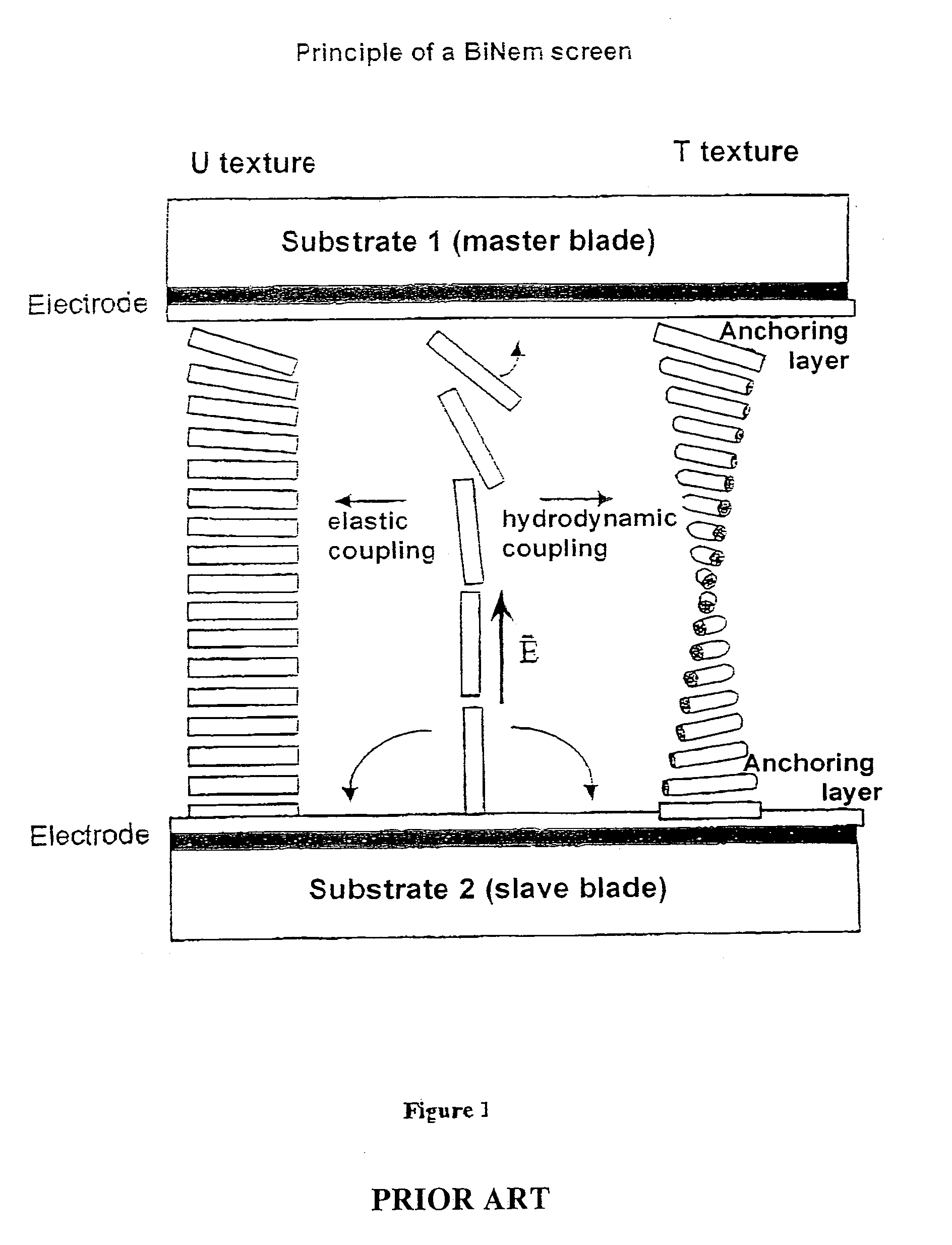
[0118]In order to demonstrate the pertinence of the invention, the optical transmission of a pixel of a BiNem screen during the addressing of an image was measured. Due to the arrangement of the polarisers, the uniform texture given in this case was the white optic state, and the texture written was the black state. When the line of the pixel is addressed, the pixel is changed to a uniform texture (white state) and then it is subjected to parasite column signals f...


PUM

PropertyMeasurementUnit
relax timeaaaaaaaaaa
voltagesaaaaaaaaaa
voltageaaaaaaaaaa

Abstract

This invention concerns a process for addressing a bistable liquid crystal material screen, characterized in that it comprises at least the step consisting of applying, to the screen column electrodes, an electrical signal whose characteristics are adapted to reduce the mean quadratic voltage of the parasite pixel pulses, in order to reduce the parasitic addressing optical effects.

Description

FIELD OF THE INVENTION[0001]This invention concerns the field of liquid crystal display devices and more specifically a process and device for controlling the switching between two states of a multiplexed bistable nematic display unit.DESCRIPTION OF THE RELATED ART[0002]The purpose of the invention is to optimise the electronic line and column addressing signals of a multiplexed bistable display unit in order to eliminate visual disruption of an image that has already been memorised, when addressing the screen to display a new image.[0003]According to the physical nature of the liquid crystal used, nematic, cholesteric, smectic, ferro-electric, etc. devices can be distinguished. In the nematic display units, which are the subject of this invention, a nematic, achiral or chiralised element is used for example, using a chiral doping agent. In this way, a spontaneously uniform or slightly twisted texture is obtained, whose thread pitch is slightly bigger than a few micrometers. The ori...

Claims


Application Information

Patent Timeline
Patent Type & Authority Patents(United States)
IPC IPC(8): G09G3/36G02F1/139G02F1/133
CPCG02F1/1391G09G3/3629G09G2320/0209G09G2310/06G09G2310/066G09G2300/0486G09G3/36
Inventor ANGELE, JACQUESVERCELLETTO, ROMAINELBHAR, THIERRY
Owner NEMOPTIC
Learn More