Driver circuit and driving method for semiconductor laser

a driving method and semiconductor laser technology, applied in semiconductor lasers, laser details, laser output parameters control, etc., can solve the problem of limiting the ability of this method to cope with a high transmission speed, the more difficult it becomes to accurately and reliably supply the pre-bias current immediately before and immediately after

Inactive Publication Date: 2007-01-02
FUJITSU LTD
View PDF10 Cites 8 Cited by
  • Summary
  • Abstract
  • Description
  • Claims
  • Application Information

AI Technical Summary

Benefits of technology

[0025]With such a construction, the second bias current is changed following the temperature characteristics of the semiconductor laser. Therefore, the output of burst data can be more accurately performed.
[0026]Furthermore, in a specific construction for the abovementioned driver circuit for a semiconductor laser, the signal processing means may generate the second bias current control signal which rises more rapidly, by a time corresponding to a predetermined bit number or a predetermined byte number, than the rise of burst data included in the...

Problems solved by technology

However, in the abovementioned known driving methods, there are the following problems.
In the driving method shown in FIG. 3, if an oscillation delay time of the LD is considered, there is a possibility that this method cannot cope with a high transmission speed.
In the current situation, it is a limit for this method to cope with a transmission speed of around 100˜200 Mb/s.
Furthermore, in the driving method shown in FIG. 4, the higher the transmission speed becomes, the more difficult it becomes to accurately and reliably supply the pre-bias current immediately before and immediately after generating an optical output of “1” level.
More specifically, the realization of a circuit or the like for determining the timing for the pre-bias current is difficult.
Moreover, in the driving method shown ...

Method used


Image

  • Driver circuit and driving method for semiconductor laser
  • Driver circuit and driving method for semiconductor laser
  • Driver circuit and driving method for semiconductor laser

Examples


first embodiment

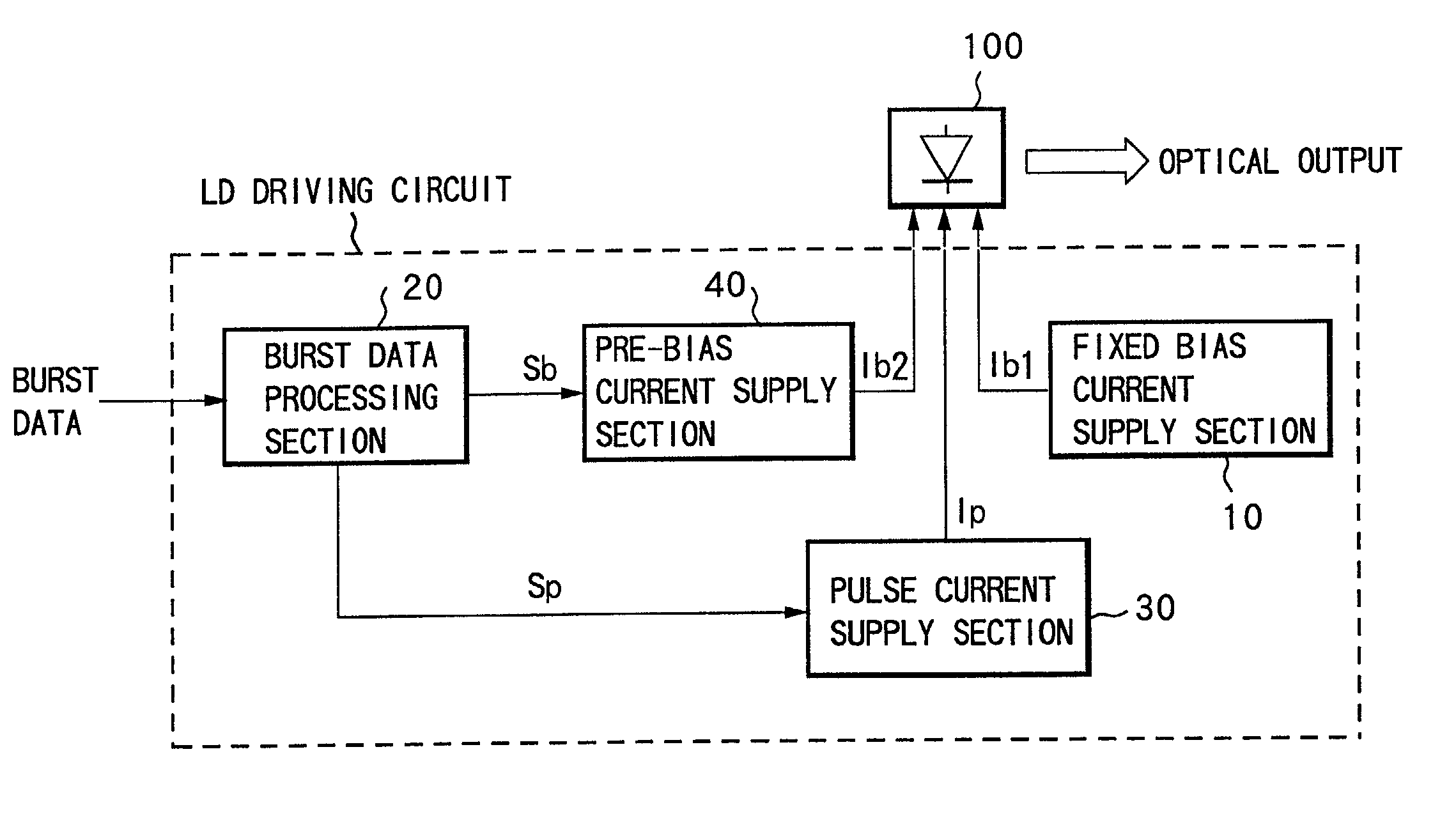
[0053]FIG. 6 is a block diagram showing a basic construction of a semiconductor laser driver circuit according to a

[0054]In FIG. 6, this driver circuit comprises: a fixed bias current supply section 10 serving as first bias current supply means that applies a fixed bias current Ib1 (first bias current) to a semiconductor laser (LD) 100, a burst data processing section 20 serving as a signal processing means that generates, based on burst data (a data signal) from outside, a pre-bias signal Sb corresponding to a second bias current control signal and a pulse signal Sp corresponding to a pulse current control signal, a pulse current supply section 30 serving as pulse current supply means that applies to the LD 100 a pulse current Ip generated in accordance with the pulse signal Sp, and a pre-bias current supply section 40 serving as second bias current control means that applies to the LD 100 pre-bias current Ib2 (second bias current) generated in accordance with the pre-bias signal S...

third embodiment

[0084]FIG. 14 is a block diagram showing a construction of an LD driving circuit of the

[0085]In FIG. 14, this LD driving circuit is constructed so that a monitor light receiving section 60 serving as optical output detection means, and a fixed bias current control section 70 serving as first bias current control means, are added to the construction of the first embodiment.

[0086]The monitor light receiving section 60 receives a part of the light output from the LD 100 and generates a monitor current, to output the monitor current to the fixed bias current control section 70. The monitor light receiving section 60 is provided with a light receiving element (PD) having sufficient light reception sensitivity with respect to weak light (spontaneous emission light) emitted from the LD 100 by the supply of the fixed bias current Ib1 at the time of non-transmission of burst data. Furthermore, in a case where the monitor current output from the light receiving element does not reach a suffic...

fifth embodiment

[0096]Next is a description of the present invention.

[0097]In the abovementioned first through fourth embodiments, the pre-bias current Ib2 is supplied to the LD 100 over the whole area (period) to be transmitted with the burst data. However, in a case where the pre-bias current Ib2 is sufficiently small compared to the pulse current Ip, once transmission of burst data is started, then taking into consideration the carrier density in the LD 100, if the pre-bias current Ib2 is applied in an area of part of the head side rather than being applied to the whole burst data transmission area, the burst data can be transmitted at a high speed. In the fifth embodiment, a description is given for a specific example of the above case.

[0098]FIG. 17 is a functional block diagram showing a construction of a burst data processing section used in the fifth embodiment. The construction of parts other than the burst data processing section is the same as for the case of any of the abovementioned res...


PUM


Abstract

A driver circuit for a semiconductor laser of the invention comprises: first bias current supply means for supplying, at least at a time of non-output of data, a first bias current to an LD; signal processing means for generating a pulse current control signal in which a burst data signal is delayed, and generating a second bias current control signal which rises more rapidly by a predetermined time than the rise of burst data included in the pulse current control signal; pulse current supply means for supplying to the LD a pulse current generated in accordance with the pulse current control signal; and second bias current supply means for supplying to the LD a second bias current generated in accordance with the second bias current control signal.

Description

[0001]This application is a continuation of PCT / JP99 / 04190 filed on Aug. 3, 1999.TECHNICAL FIELD[0002]The present invention relates to a driver circuit and a driving method for a semiconductor laser, and in particular relates to a driver circuit and a driving method for a semiconductor laser suitable for when burst transmission is performed,.BACKGROUND ART[0003]Recently, optical communication networks utilizing the broadband characteristics of an optical fiber are gaining attention. For example, optical access networks where optical fibers are laid for each house as with FTTH (Fiber To The Home), for supplying multi-media services such as CATV or VOD are gaining considerable attention.[0004]FIG. 1 shows a construction of an ATM-PON (Passive Optical Network) that has gained attention as one of systems for realizing an optical access network.[0005]In FIG. 1, the ATM-PON has a basic structure where a plurality of subscriber side apparatus #1–#n are connected via an optical coupler to a...

Claims


Application Information

Patent Timeline
IPC IPC(8): H01S3/13H01S3/00H01S5/042H01S5/06H01S5/0683
CPCH01S5/042H01S5/0683H01S5/0612H01S5/0428
Inventor TOCHIO, YUJI
Owner FUJITSU LTD
Why Eureka
Try Eureka