
Etching process for micromachining crystalline materials and devices fabricated thereby

a technology of crystalline materials and micromachining, which is applied in the direction of microstructural devices, microstructural technology, liquid/fluent solid measurements, etc., can solve the problems of unacceptable reduction of the benefits of crystallographic planes, unsatisfactory dicing saw cuts, and difficult otherwise achieved assembly economics

Active Publication Date: 2007-01-02
SAMSUNG ELECTRONICS CO LTD
View PDF65 Cites 11 Cited by
  • Summary
  • Abstract
  • Description
  • Claims
  • Application Information

AI Technical Summary

Benefits of technology

This approach enables the creation of substrates with precise, intersecting optical elements that maintain crystallographic orientation, enhancing the alignment and functionality of optical microbench structures by preventing the formation of wedge-shaped end walls and allowing for deeper etching without compromising the crystallographic planes.

Problems solved by technology

Thus microsystems can be achieved with assembly economy difficult to otherwise achieve.
While discrete, non-communicating, three-dimensional structures may be conveniently formed by an anisotropic etching, etched structures which communicate with one another at particular geometries, such as a convex corner, pose significant problems for applications in which it is desirable to maintain the precise geometry defined by the crystallographic planes.
Thus, the benefits provided by the crystallographic planes can be unacceptably diminished.
However, dicing saw cuts can be undesirable, because such cuts typically must extend across the entire substrate, or consume an undesirably large portion of it, and may not conveniently be located at discrete locations within the substrate.
Moreover, dicing saw cuts create debris which may be deposited across the substrate surface and lodge within the three-dimensional structures, which may interfere with the precise positioning of optical elements within such a structure.

Method used


Image

  • Etching process for micromachining crystalline materials and devices fabricated thereby
  • Etching process for micromachining crystalline materials and devices fabricated thereby
  • Etching process for micromachining crystalline materials and devices fabricated thereby

Examples


Embodiment Construction

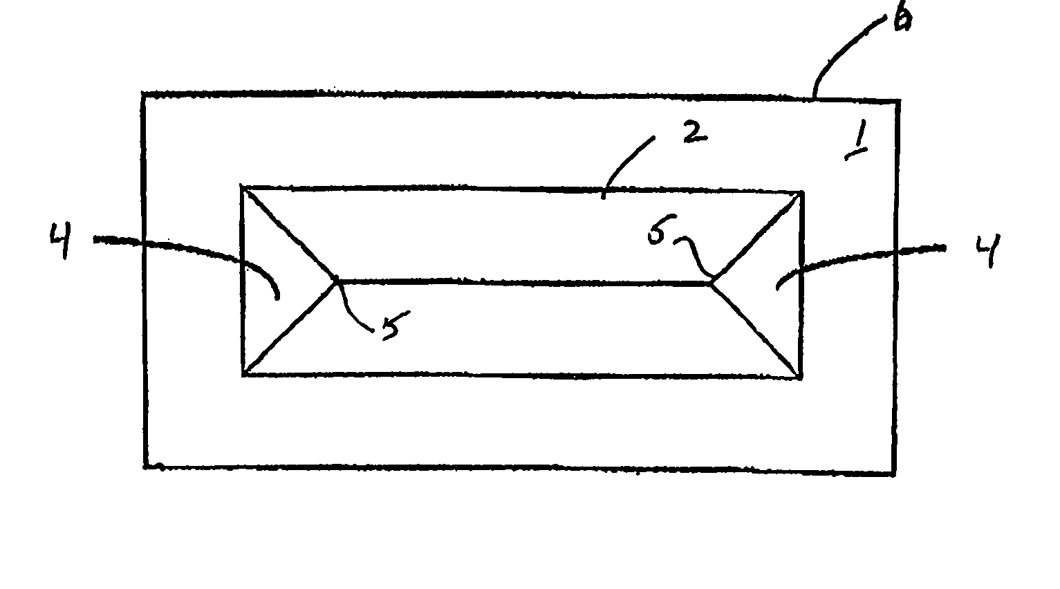
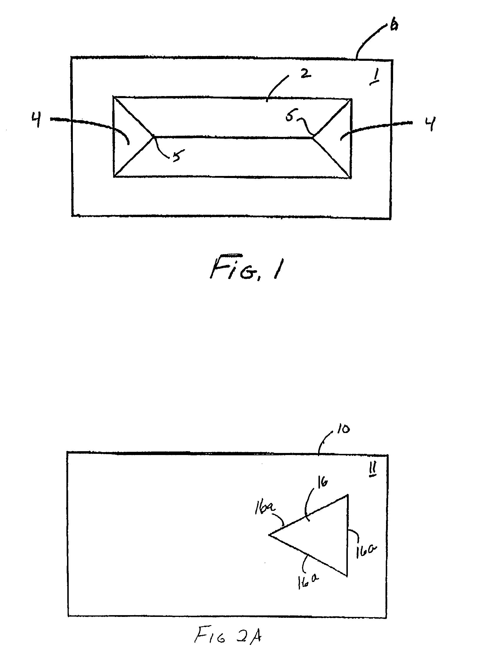
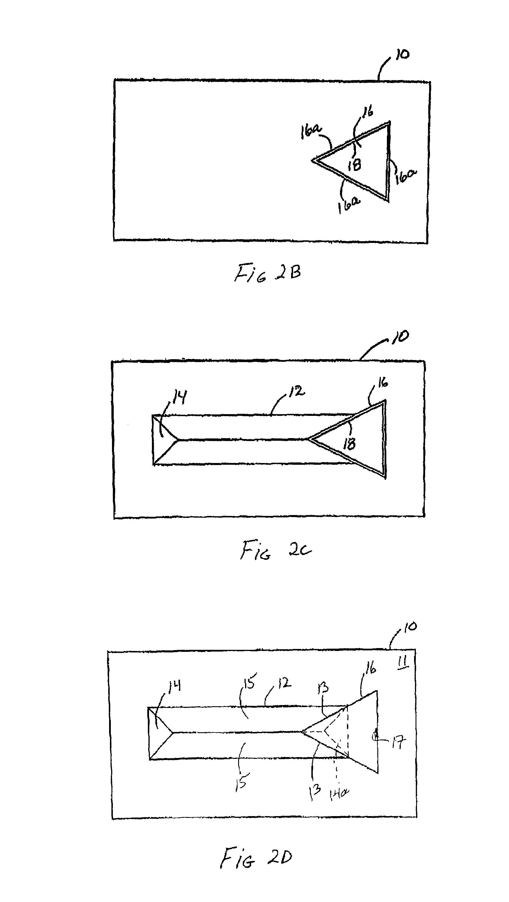
[0055]Referring now to the figures, wherein like elements are numbered alike throughout, several different embodiments of devices in accordance with the present invention are illustrated. The different embodiments include a substrate having at least two common features, an etch-stop pit and an anisotropically etched feature adjacent the etch-stop pit. The etch-stop pit has a shape suited to supporting an etch-stop layer on the surfaces of the etch-stop pit. The etch-stop pit is created prior to creating the anisotropically etched feature. The etch-stop layer comprises a material resistant to the etchant which is used to create the anisotropically etched feature. After the etch-stop layer is provided, the anisotropically etched feature is etched in the substrate. The etch-stop layer prevents the anisotropic etching from extending into the region where the etch-stop pit is located. The prevention of such anisotropic etching by the etch-stop layer provides that the crystallographic pla...


PUM

PropertyMeasurementUnit
areaaaaaaaaaaa
angleaaaaaaaaaa
aspect ratioaaaaaaaaaa

Abstract

The present invention relates generally to micromachining. More particularly, the present invention relates to a method for combining directional ion etching and anisotropic wet etching and devices and structures fabricated thereby. The present invention is particularly applicable to silicon micromachining and provides architectures that combine crystallographic surfaces and vertical dry etched surfaces together in the same structure.

Description

RELATED APPLICATIONS[0001]This application claims the benefit of priority of U.S. Provisional Application No. 60 / 472,910 filed on May 23, 2003 and U.S. Provisional Application No. 60 / 472,909 filed on May 23, 2003, the entire contents of which applications are incorporated herein by reference. This application is related to the subject matter of U.S. application Ser. No. 10 / 860,811 filed on May 24, 2004.FIELD OF THE INVENTION[0002]The present invention relates generally to micromachining. More particularly, the present invention relates to a method for combining directional ion etching and anisotropic wet etching and devices and structures fabricated thereby. The present invention is particularly applicable to silicon micromachining.BACKGROUND OF THE INVENTION[0003]The art of bulk micromachining in silicon has changed since the invention of practical means to etch vertical sidewalls in silicon using dry etching technology, as has largely resulted from the invention of the BOSCH proce...

Claims


Application Information

Patent Timeline
Patent Type & Authority Patents(United States)
IPC IPC(8): B44C1/22B29D11/00C03C15/00C03C25/68C23F1/00G02B6/42B81B1/00B81C1/00H01L31/00
CPCB81C1/00547B81C1/00B81B2201/047G02B6/4214
Inventor STEINBERG, DAN A
Owner SAMSUNG ELECTRONICS CO LTD
Learn More