Semiconductor integrated circuit and test method thereof

a technology of integrated circuits and semiconductors, applied in electronic circuit testing, digital storage, instruments, etc., can solve problems such as the increase of circuit area, and achieve the effect of suppressing the increas

Inactive Publication Date: 2006-12-26
SOCIONEXT INC
View PDF5 Cites 22 Cited by
  • Summary
  • Abstract
  • Description
  • Claims
  • Application Information

AI Technical Summary

Benefits of technology

[0015]The present invention is made so as to solve above problems, and the object thereof is to provide a semiconductor integrated circuit which can suppress an increase in circuit area for redundant repair and circuit area for scan test, and a test method thereof.
[0024]According to the configuration described above, in the redundant repair circuit of the memory using the BIST, the data storage section, which retrieves the signal which has been branched from the signal inputted into the memory from the BIST, is prepared, the data storage section is used as a memory element (flip-flop) for storing the faulty address during the test of the memory, and the flip-flop in the data storage section is used as a part of the scan chain during the test of the BIST circuit itself and the peripheral logic of the memory, and thereby it becomes possible to suppress an increase in circuit area which is needed for the scan test for the logic portion and the test of the memory.

Problems solved by technology

Therefore, in order to achieve the repair processes for the memory and the scan test for the BIST, the memory element for repair process and the flip-flop for scan test are needed, so that there has been a problem that the circuit area has been increased.

Method used


Image

  • Semiconductor integrated circuit and test method thereof
  • Semiconductor integrated circuit and test method thereof
  • Semiconductor integrated circuit and test method thereof

Examples


first embodiment

(First Embodiment)

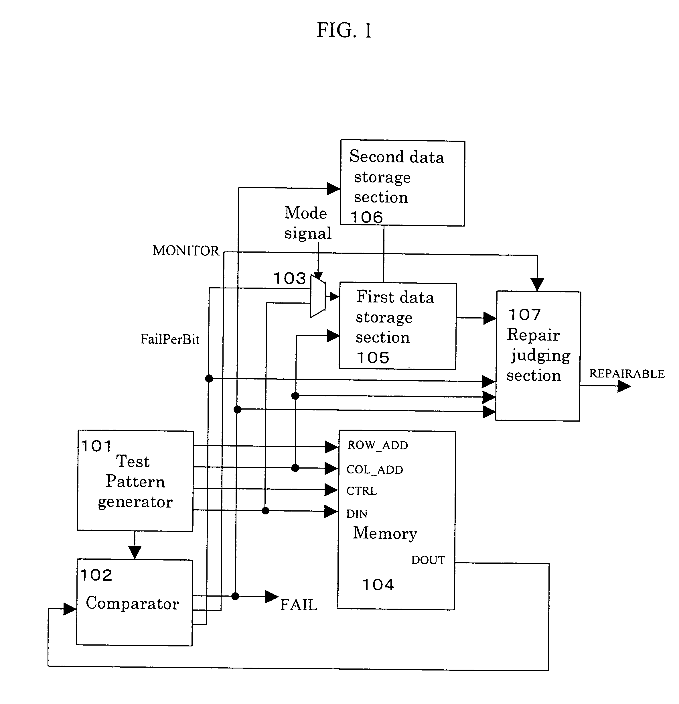
[0071]FIG. 1 is a block diagram for describing a semiconductor integrated circuit according to a first embodiment of the present invention.

[0072]A memory 104 represents a memory to be tested, which has a set of redundant lines for repair in a Column direction, and in the embodiment, includes a single Column line for repair which is replaced by the repair processes therein.

[0073]Symbol 101 represents a test pattern generating section, which generates a Row address signal ROW_ADD, a Column address signal COL_ADD, a control signal CTRL, and a data input signal DIN, and inputs them into the memory 104.

[0074]Symbol 102 represents a comparing section, which compares an output response DOUT of the memory 104 with respect to the test pattern inputted into the memory 104 with a value expected when the memory is normal (expected value), and detects a faulty cell which does not normally store the signal. The comparing section 102 generates a FAIL signal which becomes active o...

second embodiment

(Second embodiment)

[0119]FIG. 6 is a block diagram for describing a semiconductor integrated circuit according to a second embodiment of the present invention.

[0120]A memory 604 represents a memory to be tested, which has a set of redundant lines for repair in the Row direction, and in the embodiment, includes a single Row line for repair which is replaced by the repair processes therein.

[0121]Symbol 601 represents a test pattern generating section, which generates a Row address signal ROW_ADD, a Column address signal COL_ADD, a control signal CTRL, and a data input signal DIN, and inputs them into the memory 604.

[0122]Symbol 602 represents a comparing section, which compares an output response DOUT of the memory 604 with respect to the test pattern inputted into the memory 604 with a value expected when the memory is normal (expected value), and detects a faulty cell which does not normally store the signal. The comparing section 602 generates a FAIL signal which becomes active onc...

third embodiment

(Third Embodiment)

[0162]FIG. 10 is a block diagram for describing a semiconductor integrated circuit according to a third embodiment of the present invention.

[0163]A memory 1004 represents a memory to be tested, which has redundant lines for repair in a Column direction and a Row direction, and in the embodiment, includes a single Column line for repair and a single Row line for repair which are replaced by the repair processes therein.

[0164]Symbol 1001 represents a test pattern generating section, which generates a Row address signal ROW_ADD, a Column address signal COL_ADD, a control signal CTRL, and a data input signal DIN, and inputs them into the memory 1004.

[0165]Symbol 1002 represents a comparing section, which compares an output response DOUT of the memory 1004 with respect to the test pattern inputted into the memory 1004 with a value expected when the memory is normal (expected value), and detects a faulty cell which does not normally store the signal. The comparing sectio...


PUM


Abstract

A semiconductor integrated circuit includes a memory which has redundant lines for repair in both a column direction and a row direction. A test pattern generating section generates a specific test pattern for the memory. A comparing section reads an output from the memory to judge whether or not a fault cell exists in the memory and outputs a signal which shows existence or nonexistence of a faulty cell. The circuit includes a first data storage section, which operates in a first test mode for a test of the memory and a second test mode for a scan test, and a second data storage section which receives an output signal of the comparing section to store a state of presence or absence of a failure corresponding to the existence or nonexistence of the faulty cell. A repair judging section receives an input to the first data storage section and an output of retained contents in the first data storage section and judges that the memory is repairable. When the second data storage section is in a state where the failure exists, the first data storage section holds the data retained in the first data storage section.

Description

[0001]This application claims the following foreign priority document for benefit of filing date per 35 USC 119: Japanese Application. No. 2003-105990 filed Apr. 10, 2003.BACKGROUND OF THE INVENTION[0002]1. Field of the Invention[0003]The present invention relates to a semiconductor integrated circuit capable of testing a memory, in particular testing a memory having a redundant cell and testing a peripheral logic of the memory, using a Built In Self Test (BIST), and a test method thereof.[0004]2. Description of the Prior Art[0005]Recently, the number and the scale of the memories (bit width and the number of words), which have been mounted in a semiconductor integrated circuit (LSI), have been increased. According to this, the number of external pins and the test time which are needed for inspecting the memory mounted in the LSI using a circuit tester from the outside increase.[0006]In contrast to this, importance of a BIST (Built In Self Test, hereinafter referred to as BIST) tech...

Claims


Application Information

Patent Timeline
Patent Type & Authority Patents(United States)
IPC IPC(8): G11C29/44G11C29/00G11C29/12G01R31/28
CPCG11C29/44G11C29/4401G11C2029/0405G11C2029/1208
Inventor ICHIKAWA, OSAMU
Owner SOCIONEXT INC
Why Eureka
Try Eureka