Semiconductor device
a semiconductor device and semiconductor technology, applied in the direction of solid-state devices, basic electric elements, electrical apparatus construction details, etc., can solve the problems of increasing ground electric noise, increasing manufacturing costs of semiconductor devices, and insufficient reduction of noise when operation becomes faster, so as to reduce electrical noise, reduce noise, and perform high-speed transmission
- Summary
- Abstract
- Description
- Claims
- Application Information
AI Technical Summary
Benefits of technology
Problems solved by technology
Method used
Image
Examples
embodiment 1
[0074 will be described in detail below.
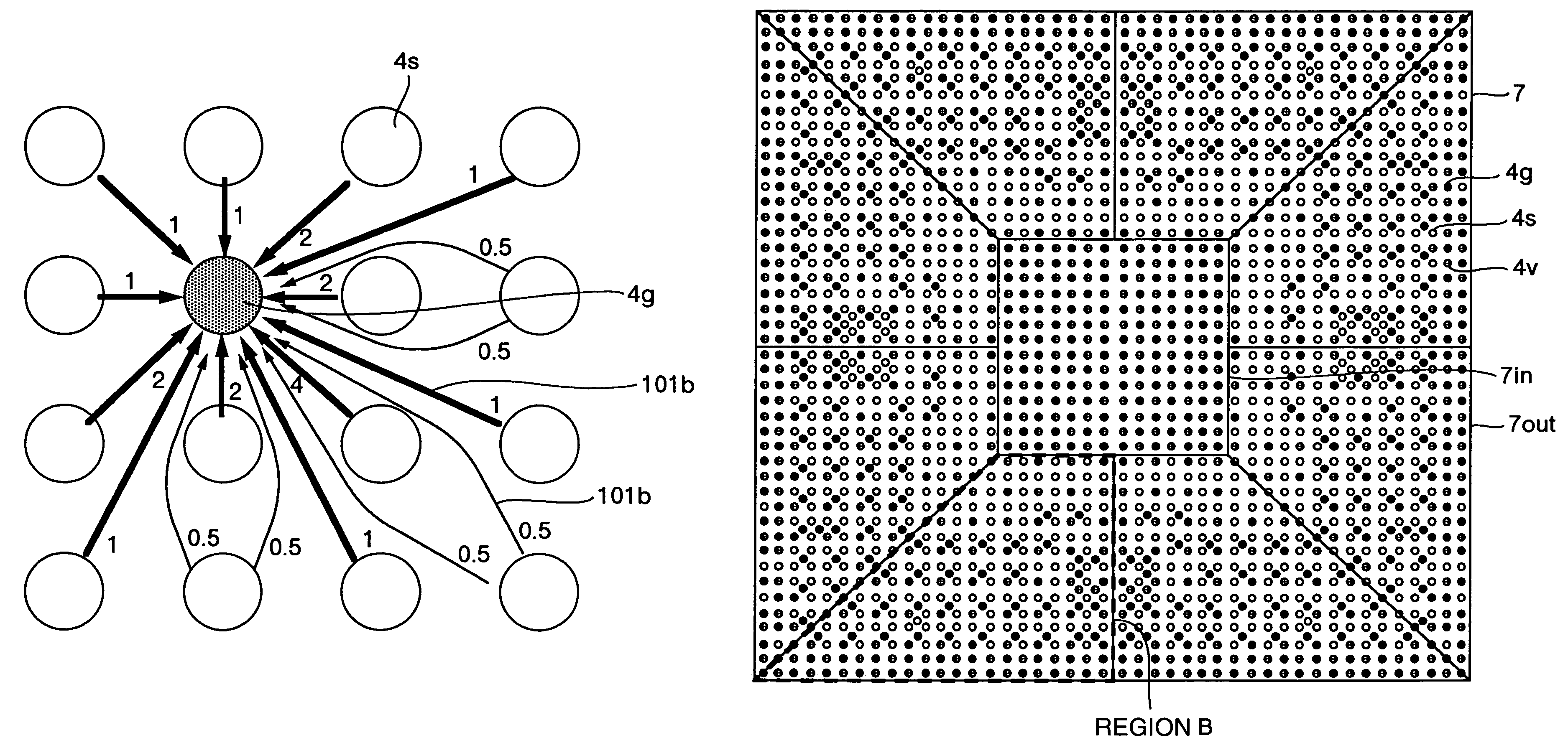
[0075]FIG. 8 illustrates a layout of through holes in the core layer 7. The through holes 4 of the core layer 7 are disposed in a grid, and nonconsecutive through holes are disposed on boundaries between regions. The through hole grids are divided into an inside where potential is low and an outside where potential is high depending on the difference of potential of the power through hole. An inner through hole grid region is an inner power region 7in, while a through hole grid region outside the inner power region 7in is an outer signal region 7out. In the inner power region 7in, the through hole 4v and ground through hole 4g are alternately disposed adjacent to each other. In the outer signal region 7out, through holes which do not correspond to external terminals are provided between the grids of the through holes and are connected to the conductor layers 54 and 55 which are on or under the core layer, respectively.
[0076]A trapezoidal and g...
embodiment 2
[0094 will be described below.
[0095]Embodiment 2 may be identically configured with Embodiment 1. FIG. 13 shows Embodiment 2 of the BGA semiconductor device in which the layout of through holes of core layer is different. The core layer region B includes a high speed signal region 400, as shown in FIG. 13, which comprises a combination of the first signal units 300a, 300b, 301a, 301b and the second signal units 302a, 302b, 303a, 303b shown in FIG. 10. The ratio of signal through hole, power through hole, and ground through hole of the grid in the region is 6:1:1, which is due to the same reason as in the case of pattern region 300 in Embodiment 1. Inter-grid through holes may be included in the high-speed signal region. As FIG. 12 shows, transmission of signals to be transmitted among a CPU 400a, an SRAM 400b, an LSI 400c, and a memory 400d, which are semiconductor devices using the BGA semiconductor devices of the present embodiment, are divided into two groups depending on its use...
embodiment 3
[0098 will be described below.
[0099]Embodiment 3 may basically be configured similarly to Embodiment 1. FIG. 15 shows Embodiment 3 of the BGA semiconductor in which the layout of through holes in the core layer is different. A region B of the core layer includes a high-speed bus region 500 as shown in FIG. 15 which comprises a combination of the first signal unit including 300a, 300b, 301a, 301b, and the second signal unit including 302a, 302b, 303a, 303b. The ratio of signal through holes, power through holes, and ground through holes of the grid in the region is 6:1:1, which is due to the same reason as in the case of pattern region 300 in Embodiment 1. It should be noted that inter-grid through holes may be included in the high-speed region. As FIG. 14 shows, bus 1501a, bus 2501b, and bus 3501c for transmitting a logical set of data which is dealt in one clock by LSI1500a, LSI2500b, LSI3500c, and LSI4500d, in which the BGA semiconductor of the present Embodiment 3 is used, are di...
PUM
 Abstract
Description
Claims
Application Information
 - R&D
- Intellectual Property
- Life Sciences
- Materials
- Tech Scout
- Unparalleled Data Quality
- Higher Quality Content
- 60% Fewer Hallucinations
Browse by: Latest US Patents, China's latest patents, Technical Efficacy Thesaurus, Application Domain, Technology Topic, Popular Technical Reports.
© 2025 PatSnap. All rights reserved.Legal|Privacy policy|Modern Slavery Act Transparency Statement|Sitemap|About US| Contact US: help@patsnap.com


