Voltage dependent parameter analysis
a voltage dependent parameter and analysis method technology, applied in the field of integrated circuit design, can solve the problems of inefficiency of iterative analysis, no guarantee that the maximum voltage reduction condition of blocks along any given path was actually discovered, and limited methods
- Summary
- Abstract
- Description
- Claims
- Application Information
AI Technical Summary
Benefits of technology
Problems solved by technology
Method used
Image
Examples
example one
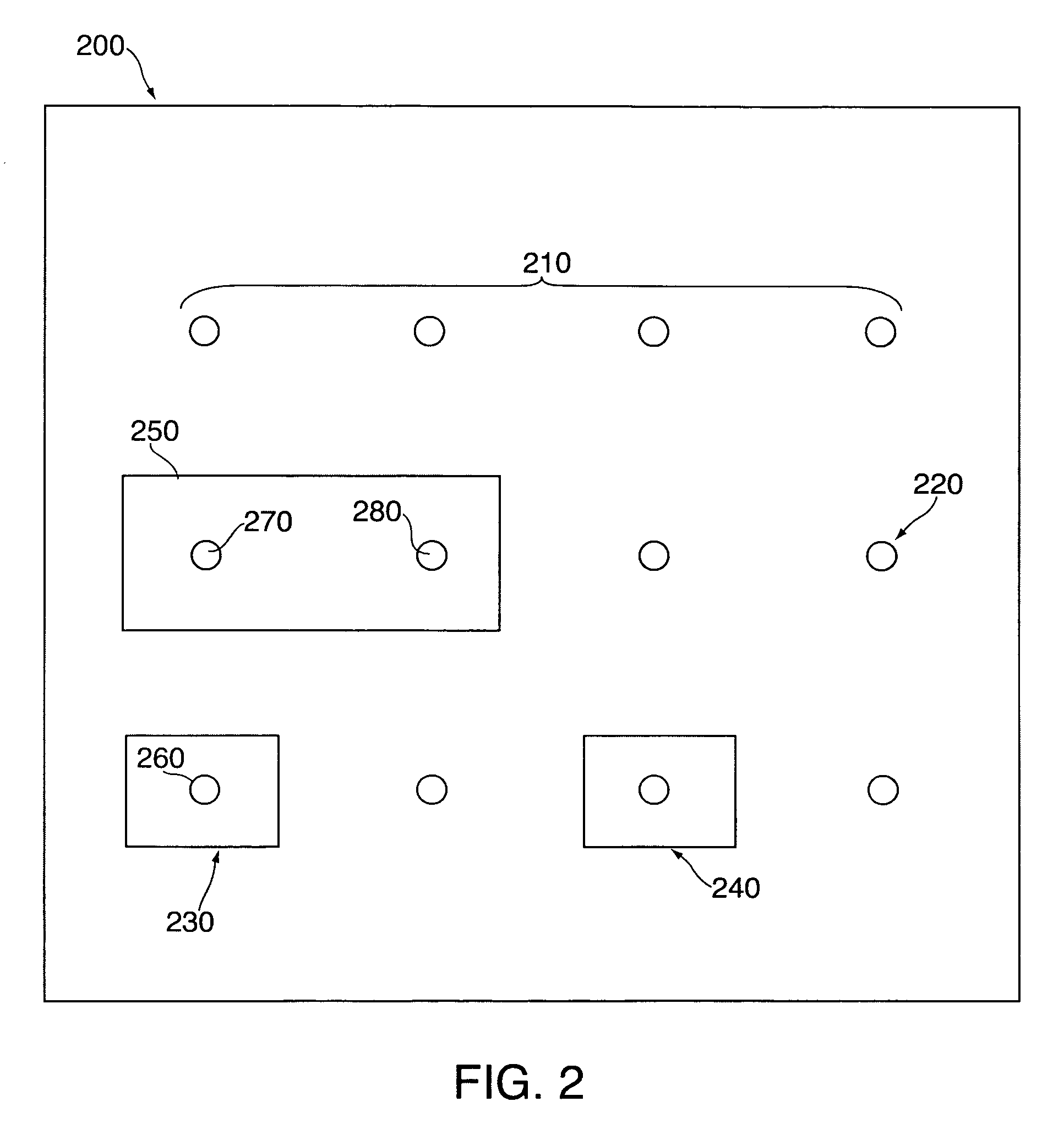
[0062]In this example, an extreme value of a voltage dependent timing parameter is determined. Referring now to FIG. 7, an example integrated circuit design 700 is illustrated. For simplicity of this example, three aggressor objects 705, 710, and 715 are shown. As discussed above, any number of aggressor objects may be identified in a given integrated circuit design. Current waveforms for each aggressor object 705, 710, and 715 are determined. FIG. 8 illustrates example current waveform 805 corresponding to aggressor object 705, current waveform 810 corresponding to aggressor object 710, and current waveform 815 corresponding to aggressor object 715. Referring again to FIG. 7, integrated circuit design 700 includes nine power bus nodes, n1,1 to n3,3. In this example, each of current waveforms 805, 810, 815 is applied to one or more power bus nodes supplying the corresponding aggressor object with power. This is done in this example with a zero applied power supply voltage. In this e...
example two
[0100]In this example, an extreme value of a voltage drop at a particular power bus node is determined. Referring again to FIG. 7, this example will use the same integrated circuit design 700 that was used in the previous example. In determining an extreme value of a voltage drop for a power bus node of an integrated circuit design, such as integrated circuit design 700, voltage waveforms corresponding to a particular power bus node and each aggressor object are determined as discussed above. For this example, the Vdrop values for power bus node n3,2 that are set forth in Table 2 will be used to determine a maximum and a minimum voltage drop value for power bus node n3,2.
[0101]In this example, a cycle period of 5.0 is used. Intervals are set in each of the voltage waveforms of FIG. 9 corresponding to node n3,2 at 0.0, 1.0, 2.0, 3.0, and 4.0. Note that an offset of 5.0 will bring the analysis to the beginning of the next cycle, and is therefore unneeded since an analysis using an off...
PUM
 Abstract
Description
Claims
Application Information
 - R&D
- Intellectual Property
- Life Sciences
- Materials
- Tech Scout
- Unparalleled Data Quality
- Higher Quality Content
- 60% Fewer Hallucinations
Browse by: Latest US Patents, China's latest patents, Technical Efficacy Thesaurus, Application Domain, Technology Topic, Popular Technical Reports.
© 2025 PatSnap. All rights reserved.Legal|Privacy policy|Modern Slavery Act Transparency Statement|Sitemap|About US| Contact US: help@patsnap.com


