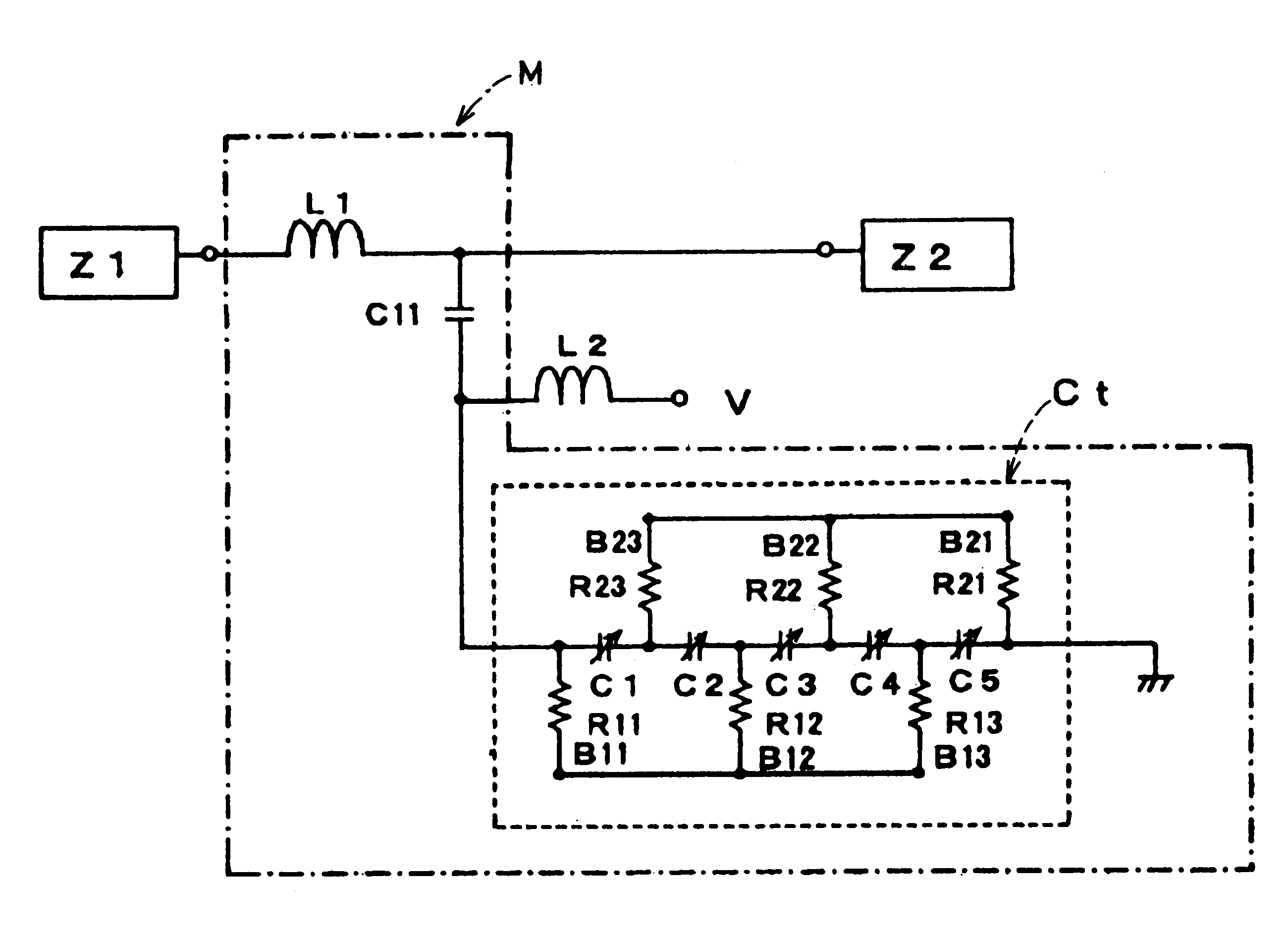
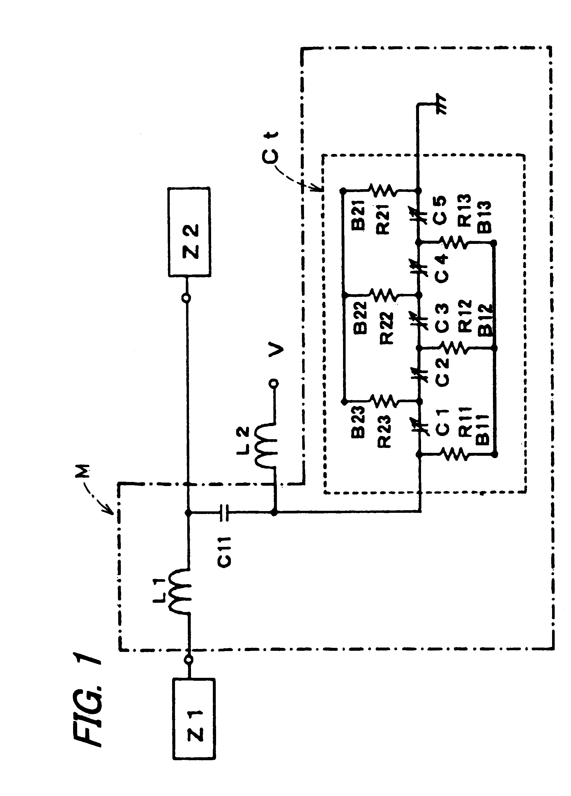
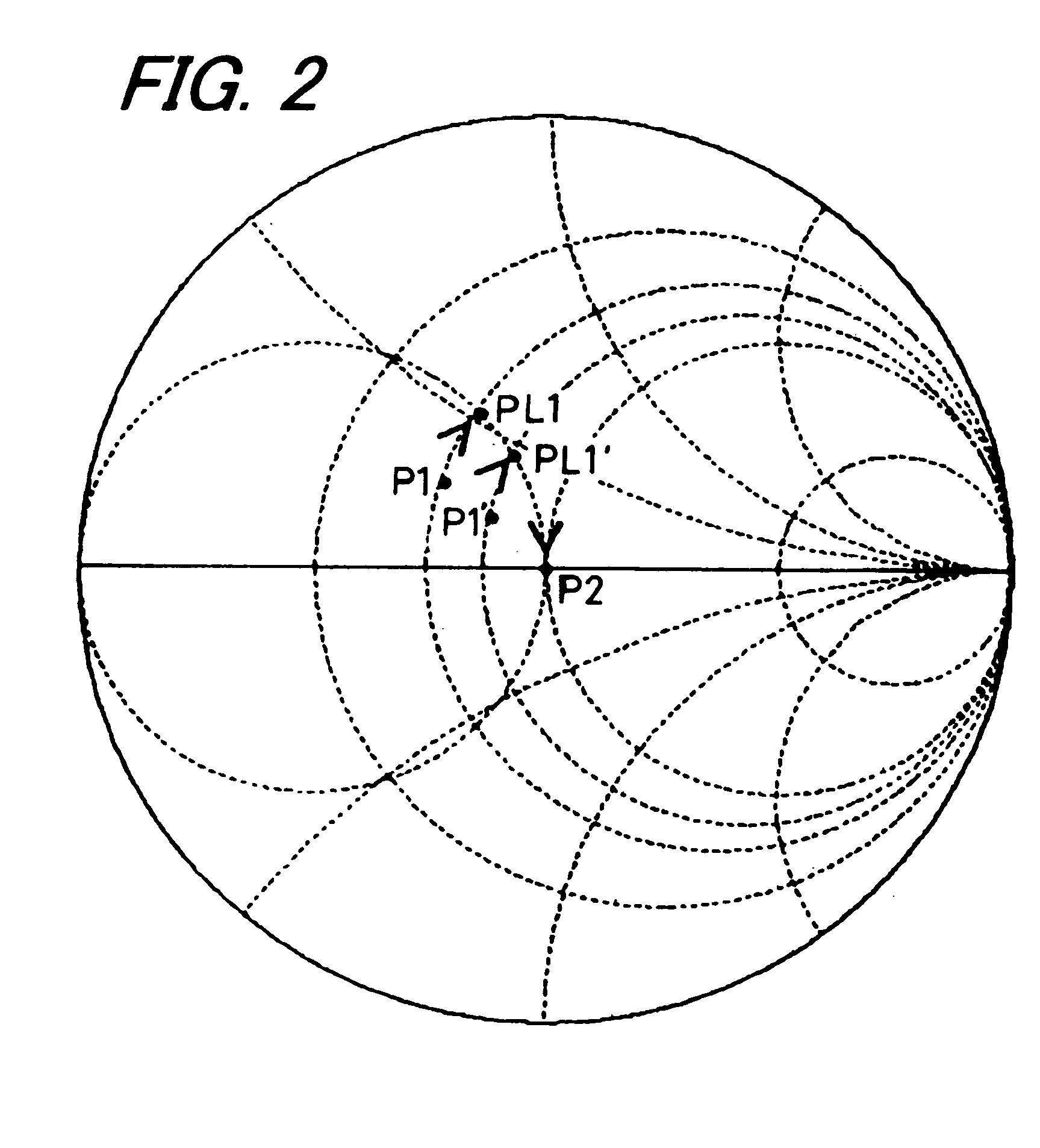
Therefore, for example, in the case of designing communication equipment using a plurality of high-frequency components, the high-frequency components are designed to have input / output impedances of 50 Ω, but there is a problem such that mismatching of the impedances occurs because of deviation of the input / output impedances of the high-frequency components from 50 Ω, or because of variations of the dimensions of the wiring patterns, interference and so on, and consequently, a characteristic desired for the communication equipment may not be obtained.
On the other hand, in the case of actually using mobile communication equipment such as a mobile terminal regulated so as to have a desired characteristic, there arises a problem such that an
electromagnetic field in the communication equipment is disturbed under the influence of a
human body holding the communication equipment when using, impedance mismatching occurs, and communication is hindered by deterioration in receiving sensitivity.
However, the variable matching circuit using the variable-capacitance
diode has a problem such that the variable matching circuit can be used only in a receiving apparatus and a receiving circuit that need small operation power, because the electric high
power handling capability of the variable-capacitance
diode is low and a
distortion characteristic due to the nonlinearity of capacitance is large.
In other words, there is a problem such that the variable matching circuit cannot be used in a transmission apparatus or a transmission circuit that need large operation power.
Additionally, the variable matching circuit has a problem such that loss at a
high frequency is large.
Further, in the variable matching circuit using the variable-capacitance capacitor as proposed in JP-A 10-335980 and JP-A 11 111566, a capacitance change of the variable-capacitance capacitor is caused also by a high-frequency
voltage, so that the variable matching circuit has a problem such that distortion characteristics such as
waveform distortion and
intermodulation distortion become large when the high-frequency voltage is high.
Further, since an
electric current easily flows to the variable-capacitance capacitor in a case of high-frequency signals, there is a problem such that the variable-capacitance capacitor generates heat and breaks down because of loss resistance while the variable-capacitance capacitor is used in a high-frequency circuit, and therefore, the electric high power handling capability of the variable matching circuit against the high-frequency signals is low.
Therefore, there is a problem such that it is necessary to design the bias supply circuit G separately from the variable matching circuit, it takes time for regulation thereof.
Moreover, there is a problem such that the circuit becomes large-sized as a whole because the variable matching circuit and the bias supply circuit G are separately formed.
The same problem occurs even if the variable-capacitance
diode is replaced with a variable-capacitance capacitor.
Still further, there is a problem such that the variable-capacitance diode 201 has a polarity for an applied voltage, and therefore, it is required to pay attention to the polarity not only when designing but also when mounting, and it takes time for mounting.
However, the conventional variable
resonance circuit using the variable-capacitance diode has a problem such that loss at a high frequency is large in the variable-capacitance diode, and therefore, loss in the entire resonance circuit becomes large, and a resonance characteristic is deteriorated.
For example, in the case of using the resonance circuit in the filter, there is a problem such that selectivity, a passing characteristic, an attenuation characteristic and so on are deteriorated by deterioration in a resonance waveform at a resonance frequency.
Moreover, in the case of using the resonance circuit in the oscillator, there is a problem such that the C / N and S / N of the oscillator are deteriorated.
Still further, the conventional variable resonance circuit using the variable-capacitance diode has a problem such that the variable resonance circuit can be used only in a receiving apparatus and a receiving circuit that need small operation power, because the electric high power handling capability of the variable-capacitance diode is low and a distortion characteristic due to the nonlinearity of capacitance is large.
In other words, there is a problem such that the variable matching circuit cannot be used in a transmission apparatus or a transmission circuit that need large operation power.
Further, in the conventional variable resonance circuit using the variable-capacitance capacitor as proposed in Japanese Unexamined Patent Publication JP-A 10-335903 (1998), a capacitance change of the variable-capacitance capacitor is caused also by a high-frequency voltage, so that the variable resonance circuit has a problem such that distortion characteristics such as
waveform distortion and
intermodulation distortion become large when the high-frequency voltage is high.
However, there is a problem such that direct
current electric field strength is also decreased when the thickness of the dielectric layer is increased, and therefore, a capacitance change rate is also decreased, and a resonance frequency variable width in the variable resonance circuit becomes small.
Further, since an
electric current easily flows to the variable-capacitance capacitor in a case of high-frequency signals, there is a problem such that the variable-capacitance capacitor generates heat and breaks down because of loss resistance while the variable-capacitance capacitor is used in a high-frequency circuit, and therefore, the electric high power handling capability of the variable resonance circuit is low.
However, there is a problem such that the direct
current electric field strength is also decreased when the thickness of the dielectric layer is increased, and therefore, a capacitance change rate is also decreased, and a resonance frequency variable width in the variable resonance circuit becomes small.
Therefore, there is a problem such that it is necessary to design the bias supply circuit G, it takes time for regulation thereof.
Moreover, there is a problem such that the circuit becomes large-sized as a whole because the variable resonance circuit and the bias supply circuit G are separately formed.
With respect to the need for the bias supply circuit C, the conventional variable resonance circuit has the same problem even if the variable-capacitance diode is replaced with a variable-capacitance capacitor.
Still further, the variable resonance circuit using the variable-capacitance diode also has a problem such that the variable-capacitance diode 201 has a polarity for an applied voltage, and therefore, it is required to pay attention to the polarity not only when designing but also when mounting, and it takes time for mounting.
However, the conventional variable phase-shifting circuit using the variable capacitance diode has a problem such that loss at a high frequency is large in the variable-capacitance diode, and therefore, loss in the entire phase-shifting circuit becomes large is deteriorated.
However, the variable phase-shifting circuit using the variable-capacitance diode has a problem such that the variable phase-shifting circuit can be used only in a receiving apparatus and a receiving circuit that need small operation power, because the electric high power handling capability of the variable-capacitance diode is low and a distortion characteristic due to the nonlinearity of capacitance is large.
In other words, there is a problem such that the variable matching circuit cannot be used in a transmission apparatus or a transmission circuit that need large operation power.
Therefore, there is a problem such that it is necessary to design the bias supply circuit G separately from the variable phase-shifting circuit, it takes time for regulation thereof.
Moreover, there is a problem such that the circuit becomes large-sized as a whole because the variable phase-shifting circuit and the bias supply circuit G are separately formed.
The same problem occurs even if the variable-capacitance diode is replaced with a variable-capacitance capacitor.
Still further, in the variable phase-shifting circuit using the variable-capacitance diode, there is a problem such that the variable-capacitance diode 201 and 202 has a polarity for an applied voltage, and therefore, it is required to pay attention to the polarity not only when designing but also when mounting, and it takes time for mounting.
Further, in the conventional variable phase-shifting circuit using the
voltage control type of dielectric varactor as proposed in JP-A 2002-528899, a capacitance change of the
voltage control type of dielectric varactor (i.e., the variable-capacitance capacitor) is caused also by a high-frequency voltage, so that the variable phase-shifting circuit has a problem such that distortion characteristics such as waveform distortion and intermodulation distortion become large when the high-frequency voltage is high.
However, there is a problem such that direct
current electric field strength is also decreased when the gap of a capacitance forming portion is increased, and therefore, a capacitance change rate is also decreased, and a variable width of the phase-shitting amount in the variable phase-shifting circuit becomes small.
Further, since an
electric current easily flows to the variable-capacitance capacitor in a case of high-frequency signals, there is a problem such that the variable-capacitance capacitor generates heat and breaks down because of loss resistance while the variable-capacitance capacitor in used in a high-frequency circuit, and therefore, the electric high power handling capability of the variable phase-shifting circuit is low.
However, there is a problem such that the direct current
electric field strength is also decreased when the gap of a capacitance forming portion is increased (i.e., the thickness of the dielectric layer is increased), and therefore, a capacitance change rate is also decreased, and variable width of the phase shifting amount in the variable phase-shifting circuit becomes small.
However, the conventional variable attenuation circuit using the variable-capacitance diode has a problem such that the electric high power handling capability of the variable-capacitance diode is low and a distortion characteristic due to the nonlinearity of capacitance is large.
Further, in the conventional variable attenuation circuit using the variable-capacitance diode, loss at a high frequency in the variable-capacitance diode is large, and therefore, for example, in a case where the variable attenuation circuit is used in a receiving circuit, the level of a reception
signal is small, and there arises a problem such that a
signal is attenuated when attenuation of the signal is not desired.
Therefore, there is a problem such that it is necessary to design the bias supply circuit G, it takes time for regulation thereof.
Moreover, there is a problem such that the circuit becomes large-sized as a whole because the variable attenuation circuit and the bias supply circuit G are separately formed.
Still further, in the variable attenuation circuit using the variable-capacitance diode, there is a problem such that the variable capacitance diode 201 has a polarity for an applied voltage, and therefore, it is required to pay attention to the polarity not only when designing but also when mounting, and it takes time for mounting.


