
Method and apparatus to increase strain effect in a transistor channel

a transistor channel and strain effect technology, applied in the direction of electrical equipment, semiconductor devices, basic electric elements, etc., can solve the problems of increasing the mobility of carriers and limiting the speed of improved devices, and achieve the effect of enhancing stress in semiconductor devices

Active Publication Date: 2006-10-10
GLOBALFOUNDRIES U S INC
View PDF108 Cites 22 Cited by
  • Summary
  • Abstract
  • Description
  • Claims
  • Application Information

AI Technical Summary

Benefits of technology

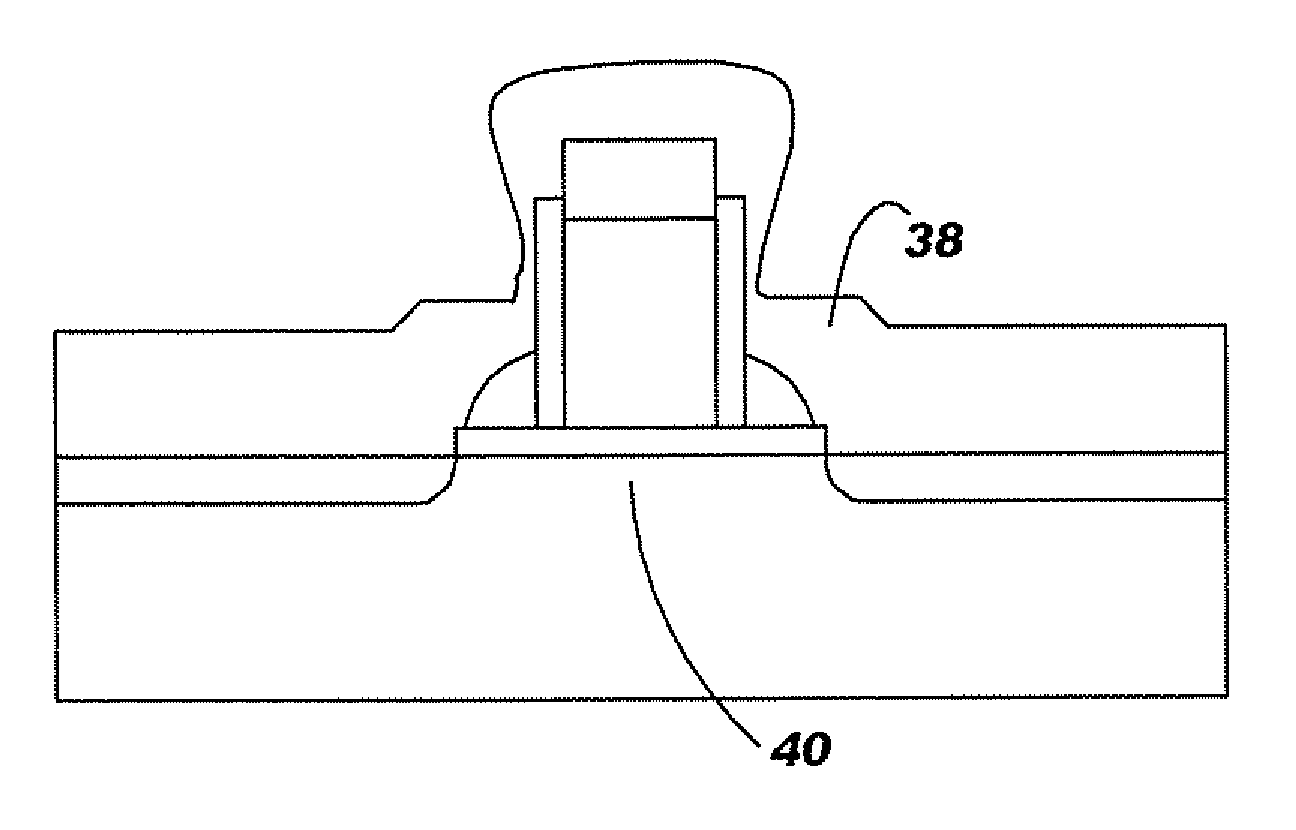
The invention is a method of enhancing stress in a semiconductor device by depositing a nitride film on the substrate and gate stack, making it thicker over the substrate and thinner over the gate stack. This results in a stressed nitride film that enhances the performance of the semiconductor device. The invention also includes a semiconductor device with a stressed nitride film that is thicker over the substrate and thinner over the gate stack.

Problems solved by technology

As semiconductor devices shrink, carrier mobility has become a roadblock for improved device speed.

Method used


Image

  • Method and apparatus to increase strain effect in a transistor channel
  • Method and apparatus to increase strain effect in a transistor channel
  • Method and apparatus to increase strain effect in a transistor channel

Examples


Embodiment Construction

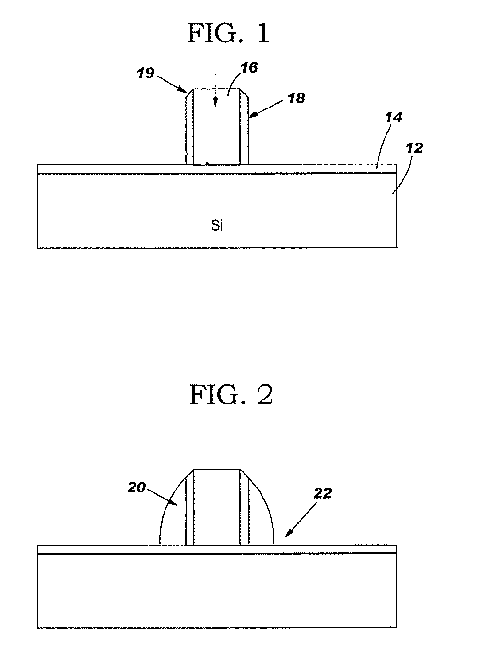
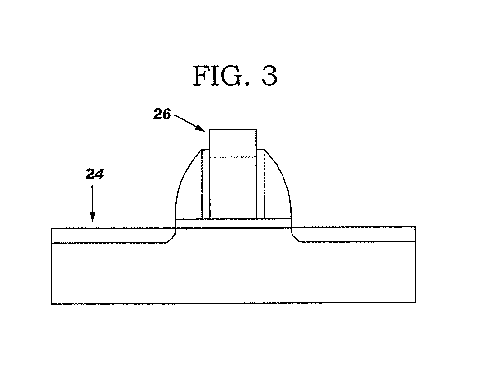
[0024]Transistor performance may be enhanced by creating stress in the transistor channel region. Accordingly, a gate structure may be made so that an enhanced stress is induced in the transistor channel from a stressed nitride film. To achieve this enhanced strain effect, one embodiment of the invention includes removing the gate spacer from the wafer after salicide is formed and then depositing a non-conformal Si3N4 film including forming little or no nitride on gate sidewalls at the top of the gate stack. In this manner, enhancement of transistor performance is provided by creating a desired stress in the transistor channel region of the device. It should be noted that this method and apparatus to increase strain effect in a channel of a transistor works for both n-type or p-type devices. As such, the nitride may be made either tensile or compressive by suitably adjusting the deposition parameters as is well known in the art.

[0025]In other embodiments, this structure may be obtai...


PUM

PropertyMeasurementUnit
compressive stressesaaaaaaaaaa
tensile stressesaaaaaaaaaa
stressaaaaaaaaaa

Abstract

A semiconductor device having a transistor channel with an enhanced stress is provided. To achieve the enhanced stress transistor channel, a nitride film is preferentially formed on the device substrate with little to no nitride on a portion of the gate stack. The nitride film may be preferentially deposited only on the silicon substrate in a non-conformal layer, where little to no nitride is deposited on the upper portions of the gate stack. The nitride film may also be uniformly deposited on the silicon substrate and gate stack in a conformal layer, with the nitride film proximate the upper regions of the gate stack preferentially removed in a later step. In some embodiments, nitride near the top of the gate stack is removed by removing the upper portion of the gate stack. In any of the methods, stress in the transistor channel is enhanced by minimizing nitride deposited on the gate stack, while having nitride deposited on the substrate.

Description

BACKGROUND OF INVENTION[0001]The invention generally relates to the enhancement of transistor performance, and more particularly to the enhancement of transistor performance by creating a desired stress in the transistor channel region.[0002]As semiconductor devices shrink, carrier mobility has become a roadblock for improved device speed. Studies have shown that electron mobility can be increased significantly by creating tensile stress in a transistor channel, and hole mobility can be improved by creating compressive stress. Thus, to improve the characteristics of a semiconductor device, tensile and / or compressive stresses are created in the channel of the n-type devices (e.g., nFETs) and / or p-type devices (e.g., pFETs). Additionally, the higher the stress in the channel, the higher mobility improvement which may be realized.[0003]The channel stress may be induced by a Si3N4 or nitride film deposited on top of the transistor. The induced stress in the channel has the same sign (te...

Claims


Application Information

Patent Timeline
Patent Type & Authority Patents(United States)
IPC IPC(8): H01L21/3205H01L21/4763H01L21/336
CPCH01L29/6653H01L29/7842H01L29/66545
Inventor YANG, HAINING S.ZHU, HUILONG
Owner GLOBALFOUNDRIES U S INC
Learn More