Semiconductor integrated circuit and level conversion circuit
a technology of integrated circuits and semiconductors, applied in the direction of logic circuits, pulse automatic control, pulse techniques, etc., can solve the problems of improper functioning of the internal circuit of the semiconductor integrated circuit, and achieve the effects of preventing the small amplitude of the input signal, reducing the amplification gain, and preventing the increase of power consumption
- Summary
- Abstract
- Description
- Claims
- Application Information
AI Technical Summary
Benefits of technology
Problems solved by technology
Method used
Image

Examples
first embodiment
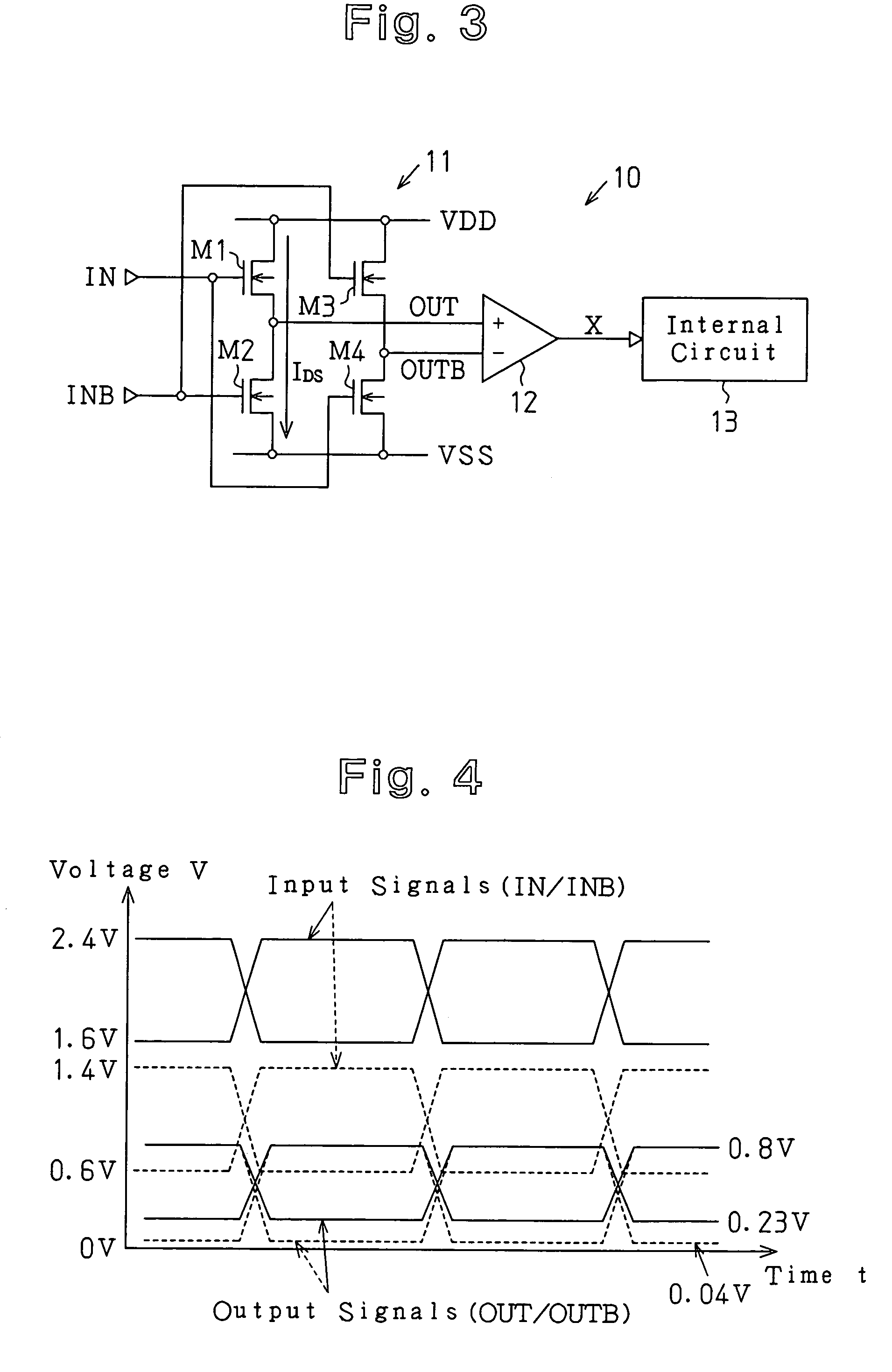
[0031]A semiconductor integrated circuit 10 according to a first embodiment of the present invention will now be discussed with reference to FIGS. 3 to 6. FIG. 3 is a schematic circuit diagram showing a semiconductor integrated circuit 10 of the first embodiment.
[0032]The semiconductor integrated circuit 10 includes a level conversion circuit 11 and a differential amplification circuit 12 which function as an input circuit in this first embodiment. The level conversion circuit 11 and the differential amplification circuit 12 converts input signals IN and INB, for example, which are provided from an external device, to a signal X having a voltage level corresponding to the operational power supply of an internal circuit 13.
[0033]The level conversion circuit 11 includes first to fourth MOS transistors M1 to M4. Each of the MOS transistors M1 to M4 is an N-type conduction transistor. In the level conversion circuit 11, the first and second MOS transistor M1 and M2 are connected in seri...
second embodiment
[0067]A semiconductor integrated circuit 10 according to a second embodiment of the present invention will now be discussed.
[0068]FIG. 7 shows a level conversion circuit 11a and a differential amplification circuit 12a incorporated in the semiconductor integrated circuit 10.
[0069]In the same manner as in the first embodiment, the level conversion circuit 11a of the second embodiment includes first to fourth MOS transistors M1 to M4. However, the MOS transistors M1 to M4 differ from those of the first embodiment in that they are P-type conduction transistors.
[0070]Like the first embodiment, in the level conversion circuit 11a, the first and second MOS transistor M1 and M2 are connected in series between a first power supply VDD at which the potential is high and a second power supply VSS at which the potential is low. Further, the third and fourth MOS transistors M3 and M4 are connected in series between the first and second power supplies VDD and VSS. In each of the first to fourth ...
third embodiment
]
[0083]A semiconductor integrated circuit 10 according to a third embodiment of the present invention will now be discussed.
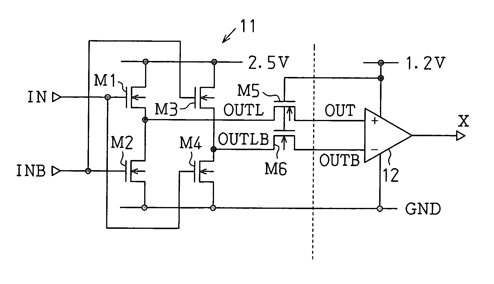
[0084]FIG. 8 shows a level conversion circuit 11 and a differential amplification circuit 12 incorporated in the semiconductor integrated circuit 10 of the third embodiment.
[0085]The level conversion circuit 11 of the third embodiment is connected to a power supply that differs from that of the differential amplification circuit 12. More specifically, the level conversion circuit 11 is connected to a first power supply at which the potential is high (2.5 V) and to a second power supply at which the potential is low (0 V). The differential amplification circuit 12 is connected to a third power supply at which the potential is high (1.2 V) and to the second power supply at which the potential is low (0V).
[0086]The circuit configuration of the level conversion circuit 11 and the differential amplification circuit 12 is the same as that of the first embodiment. The...
PUM
 Abstract
Description
Claims
Application Information
 - R&D
- Intellectual Property
- Life Sciences
- Materials
- Tech Scout
- Unparalleled Data Quality
- Higher Quality Content
- 60% Fewer Hallucinations
Browse by: Latest US Patents, China's latest patents, Technical Efficacy Thesaurus, Application Domain, Technology Topic, Popular Technical Reports.
© 2025 PatSnap. All rights reserved.Legal|Privacy policy|Modern Slavery Act Transparency Statement|Sitemap|About US| Contact US: help@patsnap.com