
Liquid crystal display device and electronic apparatus

a display device and liquid crystal technology, applied in non-linear optics, instruments, optics, etc., can solve the problems of inability to accurately measure the transceiving display light and the reflective display light in the boundary area, adversely affect the alignment of liquid crystal molecules in the boundary area between the transmissive display light and the reflective display light, and achieve high quality

Inactive Publication Date: 2006-07-04
138 EAST LCD ADVANCEMENTS LTD
View PDF20 Cites 8 Cited by
  • Summary
  • Abstract
  • Description
  • Claims
  • Application Information

AI Technical Summary

Benefits of technology

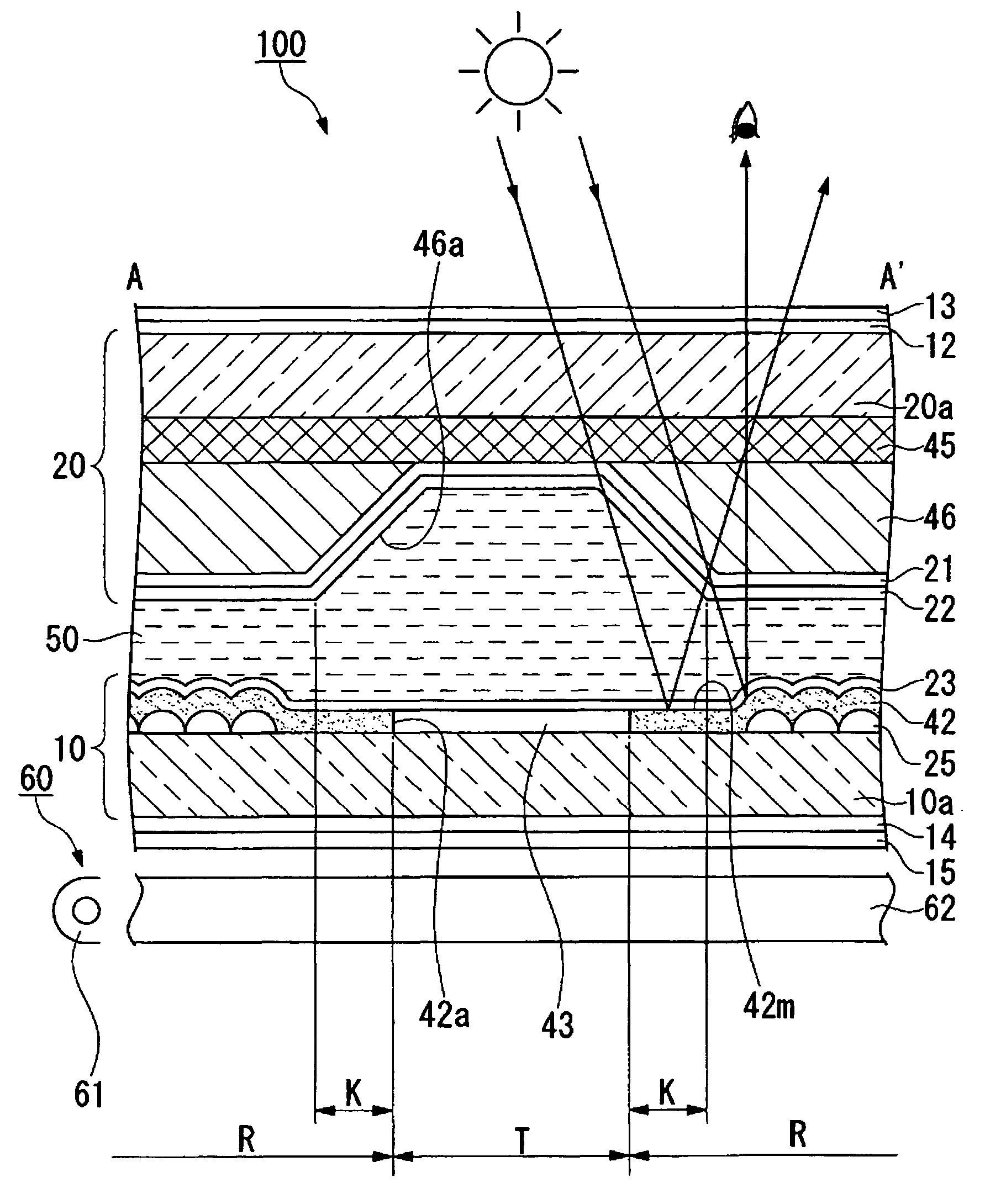
[0014]With this feature, although the boundary area is regarded as a part of the reflective display area because of having the reflective film formed therein, since the upper surface of the above-mentioned part serves as a mirror reflective surface, external light coming from the outer surface of the second substrate is regularly reflected in this boundary area. However, since when a user operates the liquid crystal display device in the usual way, the user does not see the liquid crystal display device from the regularly reflecting direction of external light such as sunlight or illuminating light, light reflected from the mirror reflective surface at the time of performing black display does not enter the eyes of the user, and therefore a contrast deterioration of the reflective display can be reduced or prevented. In addition, since the reflective film is present in the boundary area, this feature does not have an adverse affect on the transmissive display. Accordingly, in the boundary area between the reflective display area and the transmissive display area, when the thickness of the thickness-adjusting layer varies continuously and the retardation Δn·d in the boundary area varies continuously, or even when the alignment of liquid crystal molecules is disturbed, high-contrast display for both the transmissive display and the reflective display can be achieved.
[0016]When the thickness-adjusting layer is formed by a photosensitive resin as described with regard to the related art, the edge of the aperture of the thickness-adjusting layer, that is, the boundary area between the transmissive display area and the reflective display area, sometimes constitutes a tapered surface depending on the situation of a photolithography step. In this case, as the thickness of the liquid crystal layer varies continuously, the retardation Δn·d varies continuously. Even in such a case, the above structure prevents a contrast deterioration of the reflective display, thereby achieving high-contrast display for both the transmissive display and the reflective display.
[0018]With this structure, since the reflective film has the light scattering device on the upper surface except the portions serving as the mirror reflective surface, that is, the area which contributes effectively to the reflective display, the reflected light is scattered and sufficient amount of light entering the eyes of the user can be secured, thereby achieving a brighter reflective display.
[0020]With this structure, a transflective liquid crystal display device performing color display can be achieved.
[0021]An electronic apparatus according to the present invention includes the liquid crystal display device according to the present invention. With this structure, an electronic apparatus allowing selection between transmissive display and reflective display and performing high quality color display can be provided.

Problems solved by technology

As a result, in the boundary area between the transmissive display area and the reflective display area, the thickness of the liquid crystal layer varies continuously, and therefore the retardation Δn·d thereof also varies continuously, resulting in an inappropriate value for both the transmissive display light and the reflective display light in the boundary area.
Also, although the initial alignment state of liquid crystal molecules constituting the liquid crystal layer is defined by alignment films respectively disposed on the upper and lower substrates, since the aligning regulatory force of the alignment films acts at an angle on the liquid crystal molecules lying in the boundary area in which the tapered surface is disposed, the alignment of the liquid crystal molecules is adversely affected in this area.
Alternatively, even when the edge of the aperture of the thickness-adjusting layer, that is, the boundary area between the transmissive display area and the reflective display area is formed so as to have a step perpendicular to the surfaces of the substrates instead of having a tapered surface, the alignment of the liquid crystal molecules is adversely affected in the boundary area between the transmissive display area and the reflective display area.
However, the above-mentioned disturbance actually causes leakage of light in the boundary area between the transmissive display area and the reflective display area, thereby leading to a deteriorated contrast.

Method used


Image

  • Liquid crystal display device and electronic apparatus
  • Liquid crystal display device and electronic apparatus
  • Liquid crystal display device and electronic apparatus

Examples


first exemplary embodiment

[0031]A first exemplary embodiment of the present invention is described below with reference to FIGS. 1 to 5.

[0032]In this exemplary embodiment, an active-matrix, transflective liquid crystal display device of a reflector built-in type in which pixel electrodes on an element substrate serve also as a reflector is described below by way of example. FIG. 1 is a plan view of a liquid crystal display device according to this exemplary embodiment and its components, viewed from a counter substrate, and FIG. 2 is a sectional view taken along plane H-H′ indicated in FIG. 1. FIG. 3 is a schematic circuit diagram of a variety of elements, wiring lines, and so forth of a plurality of pixels formed in a matrix manner in an image display area of an electro-optical device (i.e., the liquid crystal display device shown in FIG. 1). In each figure which will be referred to in the following description, each of the layers and the components has a different reduced scale so as to be easily viewed in...

second exemplary embodiment

[0051]Referring now to FIG. 6, a liquid crystal display device according to a second exemplary embodiment of the present invention is described below.

[0052]The liquid crystal display device according to this exemplary embodiment has the same basic structure as in the first exemplary embodiment, but the color filters are disposed close to the lower substrate, and the upper substrate serves as an element substrate. Accordingly, the liquid crystal display device of the second exemplary embodiment is only different in its sectional structure from that of the first exemplary embodiment. Hence, only the sectional structure of the liquid crystal display device is described below, referring to FIG. 6 corresponding to FIG. 5. Also, the components common in FIG. 6 and FIG. 5 are denoted by the same reference characters, and the description thereof is omitted.

[0053]As shown in FIG. 6, in a liquid crystal display device 101 according to this exemplary embodiment, a lower substrate 1 has a refle...


PUM


Abstract

The invention provides a transflective liquid crystal display device which performs high-contrast display for both the transmissive display and the reflective display. A liquid crystal display device according to the present invention has transmissive a display area and a reflective display area at each dot. In addition, it has a reflective electrode disposed in the reflective display area and also has a thickness-adjusting layer to adjust a liquid crystal layer disposed therein in order to make a liquid crystal layer thinner in the reflective display area than in the transmissive display area. Also, the upper surface of an edge portion of the reflective electrode, the edge portion lying in a boundary area between the transmissive display area and the reflective display area, is arranged so as to serve as a mirror reflective surface.

Description

BACKGROUND OF THE INVENTION[0001]1. Field of Invention[0002]The present invention relates to liquid crystal display devices and electronic apparatuses. More specifically, the invention relates to a multi-gap-type transflective liquid crystal display device in which the thicknesses of a liquid crystal layer is enhanced or optimized in accordance with transmissive and reflective display areas.[0003]2. Description of Related Art[0004]Related art transflective liquid crystal display devices combining two types of display modes, such as reflective display and transmissive display modes, produce a clear display even in a dark environment while reducing power consumption. These devices achieve this by selecting the reflective mode or the transmissive mode in accordance with the level of brightness of the ambient light.[0005]Such related art transflective liquid crystal display devices include a liquid crystal display device in which a liquid crystal layer is sandwiched between upper and lo...

Claims


Application Information

Patent Timeline
IPC IPC(8): G02F1/1335G02F1/1333G02F1/1339G02F1/1343G02F1/1368
CPCG02F1/133555
Inventor MAEDA, TSUYOSHI
Owner 138 EAST LCD ADVANCEMENTS LTD
Learn More