
Versatile system for electrostatic discharge protection utilizing silicon controlled rectifier

a technology of electrostatic discharge protection and rectifier, which is applied in the direction of semiconductor devices, semiconductor/solid-state device details, transistors, etc., can solve the problems of esd damage, catastrophic (and immediate) damage, and drastically alter the electrical characteristics of semiconductor devices, etc., to minimize or eliminate scr operation latch-up problems, easy to implement, and easy to use

Inactive Publication Date: 2006-06-13
TEXAS INSTR INC
View PDF1 Cites 2 Cited by
  • Summary
  • Abstract
  • Description
  • Claims
  • Application Information

AI Technical Summary

Benefits of technology

This solution effectively minimizes or eliminates operational latch-up problems in semiconductor devices, ensuring reliable performance and reducing the risk of damage, while maintaining effective ESD protection across a range of voltage levels.

Problems solved by technology

For some time now, the phenomenon of electrostatic discharge (ESD) has created a number of problems for manufacturers and end-users of semiconductor technology.
ESD events can drastically alter or damage the electrical characteristics of a semiconductor device—degrading or destroying it.
Damage caused by ESD can be catastrophic (and immediate) or latent in nature.
Latent defects can result in a number of reliability and repair problems in end equipment use.
Whether ESD-induced damage is immediate or latent in nature, a damaged device is usually scrapped or replaced.
Thus, even where ESD events occur only infrequently, losses can—over time—be substantial.
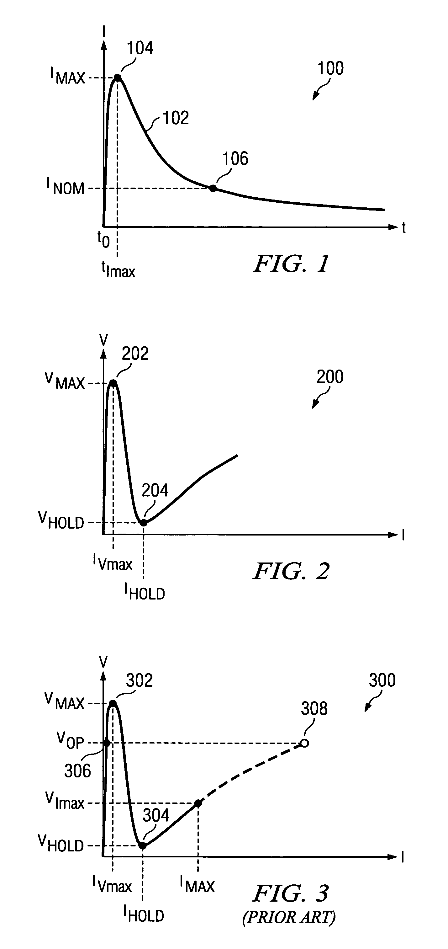
Unfortunately, however, many conventional SCR structures can experience latch-up problems during normal operation of the device in which the SCR is implemented.
Thus, minor signal noise or electrical stress can push the device past the threshold and into a hold-state latch-up.
This can cause the device to latch up, negatively impacting device and system performance.

Method used


Image

  • Versatile system for electrostatic discharge protection utilizing silicon controlled rectifier
  • Versatile system for electrostatic discharge protection utilizing silicon controlled rectifier
  • Versatile system for electrostatic discharge protection utilizing silicon controlled rectifier

Examples


Embodiment Construction

[0024]While the making and using of various embodiments of the present invention are discussed in detail below, it should be appreciated that the present invention provides many applicable inventive concepts, which can be embodied in a wide variety of specific contexts. The invention will now be described in conjunction with the manufacture of semiconductor devices utilizing silicon-controlled rectifiers (SCRs) to provide electrostatic discharge (ESD) protection. The specific embodiments discussed herein are merely illustrative of specific ways to make and use the invention and do not limit the scope of the invention.

[0025]The present invention provides a versatile system for electrostatic discharge protection utilizing SCR structures. SCR structures, according to the present invention, are provided with clamping or switching constructs. These constructs alter the behavioral characteristics of an SCR structure during normal device operation. The SCR structures of the present inventi...


PUM


Abstract

The present invention provides a system for electrostatic discharge protection in a semiconductor device, utilizing a silicon-controlled rectifier (502). The system includes the silicon controlled rectifier, which has a first p-type region (508) coupled to a voltage node (504), a first n-type region (512) having a first side adjoining the first p-type region, a second p-type region (510) having a first side adjoining a second side of the first n-type region, and a second n-type region (514) having a first side adjoining a second side of the second p-type region. A clamping structure (506) is intercoupled between the second n-type region and ground, to prevent the junction between the second p-type region and the second n-type region from retaining a forward bias. A switching structure (518) is intercoupled between the second p-type region and ground to ground the second p-type region during normal operation of the semiconductor device.

Description

[0001]This is a division of application Ser. No. 10 / 692,606, filed Oct. 24, 2003 now U.S. Pat. No. 6,949,800.TECHNICAL FIELD OF THE INVENTION[0002]The present invention relates generally to the field of semiconductor devices and, more particularly, to apparatus and methods providing silicon controlled rectifiers for electrostatic discharge protection.BACKGROUND OF THE INVENTION[0003]The continual demand for enhanced integrated circuit performance has resulted in, among other things, a dramatic reduction of semiconductor device geometries, and continual efforts to optimize the performance of every substructure within any semiconductor device. A number of improvements and innovations in fabrication processes, material composition, and layout of the active circuit levels of a semiconductor device have resulted in very high-density circuit designs. Increasingly dense circuit design has not only improved a number of performance characteristics, it has also increased the importance of, an...

Claims


Application Information

Patent Timeline
Patent Type & Authority Patents(United States)
IPC IPC(8): H01L21/82H01L21/332H01L23/62H01L27/02H01L29/00H01L29/74
CPCH01L27/0262
Inventor STEINHOFF, ROBERT M.
Owner TEXAS INSTR INC
Learn More