Electron beam treatment apparatus

an electron beam and treatment apparatus technology, applied in the field of electron beam treatment apparatus, can solve the problems of increasing the complexity of fabrication, affecting the accuracy of treatment results,

Inactive Publication Date: 2006-05-23
APPLIED MATERIALS INC
View PDF12 Cites 3 Cited by
  • Summary
  • Abstract
  • Description
  • Claims
  • Application Information

AI Technical Summary

Problems solved by technology

Fabrication of integrated devices (“ICs”), for example, and without limitation, semiconductor ICs, is complicated and, because of increasingly stringent requirements on device designs due to demands for greater device speed, fabrication is becoming ever more complicated.
For ICs having minimum feature sizes of 0.13 μm and below, problems of RC delay and crosstalk become significant.
However, small working distances may become problematic in certain applications such as, for example and without limitation, applications wherein 300 mm wafers are treated and including such applications wherein the wafers are heated.
In such applications, for small working distances, the anode may be so large that bowing or warping may become a problem.

Method used


Image

  • Electron beam treatment apparatus
  • Electron beam treatment apparatus
  • Electron beam treatment apparatus

Examples


Embodiment Construction

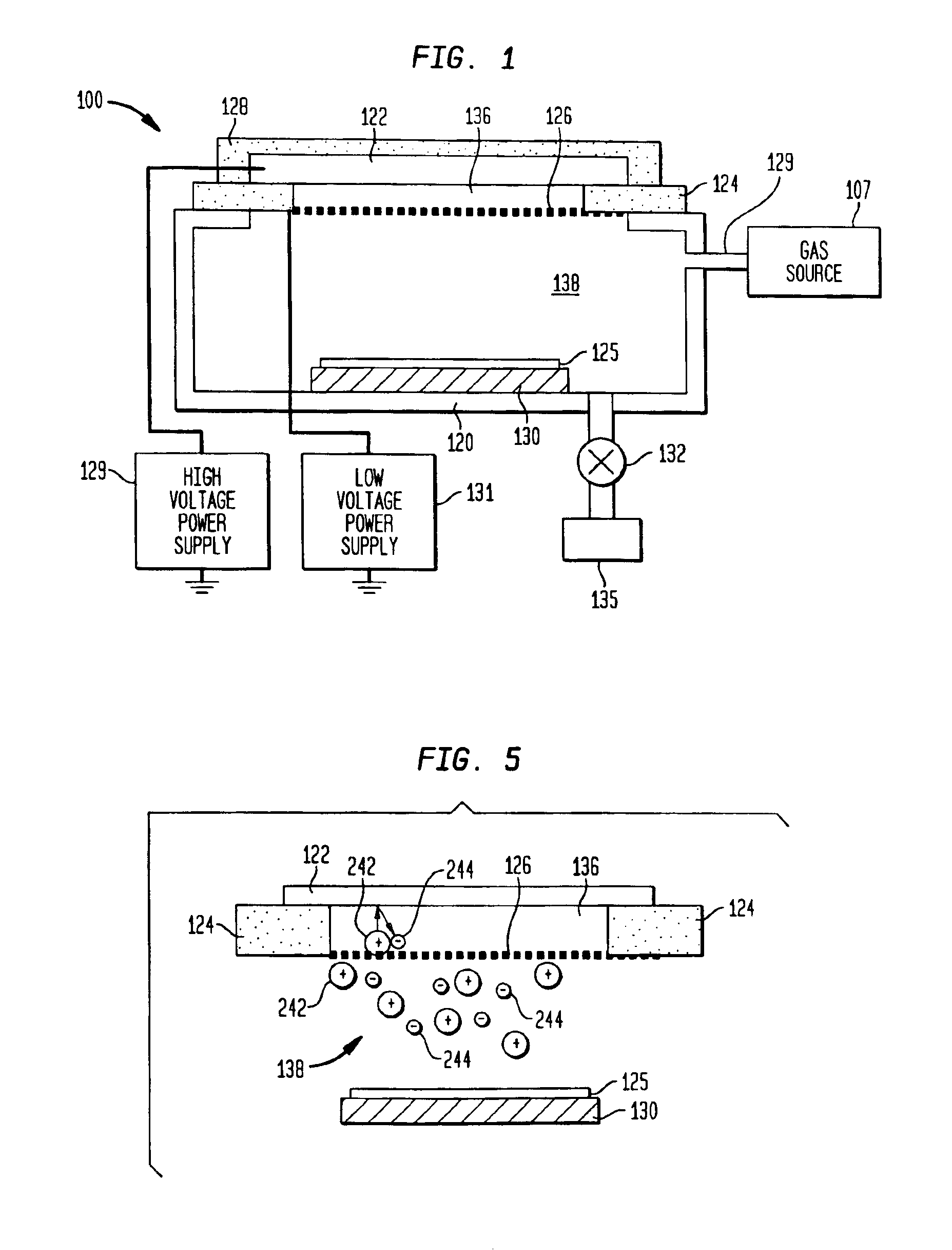
[0013]One or more embodiments of the present invention relate to electron beam treatment apparatus of the type disclosed in U.S. Pat. No. 5,003,178 (the '178 patent) that operate at values of cathode voltage, gas pressure, and working distance (i.e., a distance between the cathode and anode in a generation and acceleration region of the electron beam treatment apparatus) wherein the working distance exceeds an electron mean free path in the generation and acceleration region. As will be described in detail below, such values of cathode voltage, gas pressure, and working distance may be determined readily by one of ordinary skill in the art without undue experimentation. Co-pending patent application entitled “Improved Large Area Source for Uniform Electron Beam Generation” filed Nov. 21, 2002, Ser. No. 10 / 301,508 (which co-pending patent application and the present patent application are commonly assigned) is incorporated by reference herein.

[0014]Apparatus: FIG. 1 shows electron be...


PUM


Abstract

One embodiment of the present invention is an electron beam treatment apparatus that includes: (a) a chamber; (b) a cathode having a surface of relatively large area that is exposed to an inside of the chamber; (c) an anode having holes therein that is disposed inside the chamber and spaced apart from the cathode by a working distance; (d) a wafer holder disposed inside the chamber facing the anode; (e) a source of negative voltage whole output is applied to the cathode to provide a cathode voltage; (f) a source of voltage whose output is applied to the anode; (g) a gas inlet adapted to admit gas into the chamber at an introduction rate; and (h) a pump adapted to exhaust gas from the chamber at an exhaust rate, the introduction rate and the exhaust rate providing a gas pressure in the chamber; wherein values of cathode voltage, gas pressure, and the working distance are such that there is no arcing between the cathode and anode and the working distance is greater than an electron mean free path.

Description

TECHNICAL FIELD OF THE INVENTION[0001]One or more embodiments of the present invention pertain to apparatus for treating films using an electron beam, and methods of operating such apparatus.BACKGROUND OF THE INVENTION[0002]Fabrication of integrated devices (“ICs”), for example, and without limitation, semiconductor ICs, is complicated and, because of increasingly stringent requirements on device designs due to demands for greater device speed, fabrication is becoming ever more complicated. Today's fabrication facilities are routinely producing devices having 0.13 μm feature sizes, and tomorrow's facilities soon will be producing devices having even smaller feature sizes.[0003]For ICs having minimum feature sizes of 0.13 μm and below, problems of RC delay and crosstalk become significant. For example, device speed is limited in part by the RC delay which is determined by the resistance of metal used in an interconnect scheme and the dielectric constant of insulating dielectric mater...

Claims


Application Information

Patent Timeline
Patent Type & Authority Patents(United States)
IPC IPC(8): H01J37/30H01J37/077
CPCH01J3/025H01J37/317H01J37/077H01J37/067H01J2237/248
Inventor DEMOS, ALEXANDROS T.PONNEKANTI, HARI K.ZHAO, JUNARMER, HELEN R.
Owner APPLIED MATERIALS INC
Why Eureka
Try Eureka