
NAND flash memory device and method of reading the same

a technology of nand flash memory and morphological configuration, which is applied in the direction of digital storage, instruments, transistors, etc., can solve the problems of inability to shrink down the morphological configuration of the nand flash memory device, inability to read the same, so as to increase the source-side resistance of selection transistors and reduce leakage currents

Active Publication Date: 2006-04-25
STMICROELECTRONICS SRL +1
View PDF6 Cites 36 Cited by
  • Summary
  • Abstract
  • Description
  • Claims
  • Application Information

AI Technical Summary

Benefits of technology

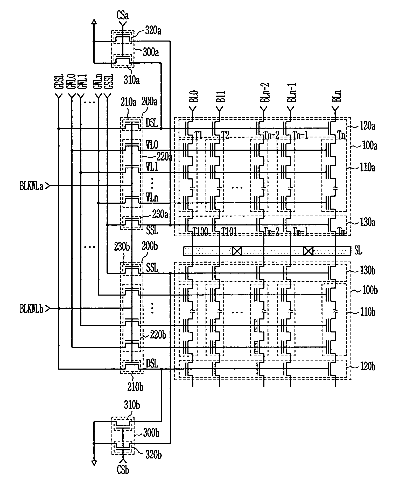
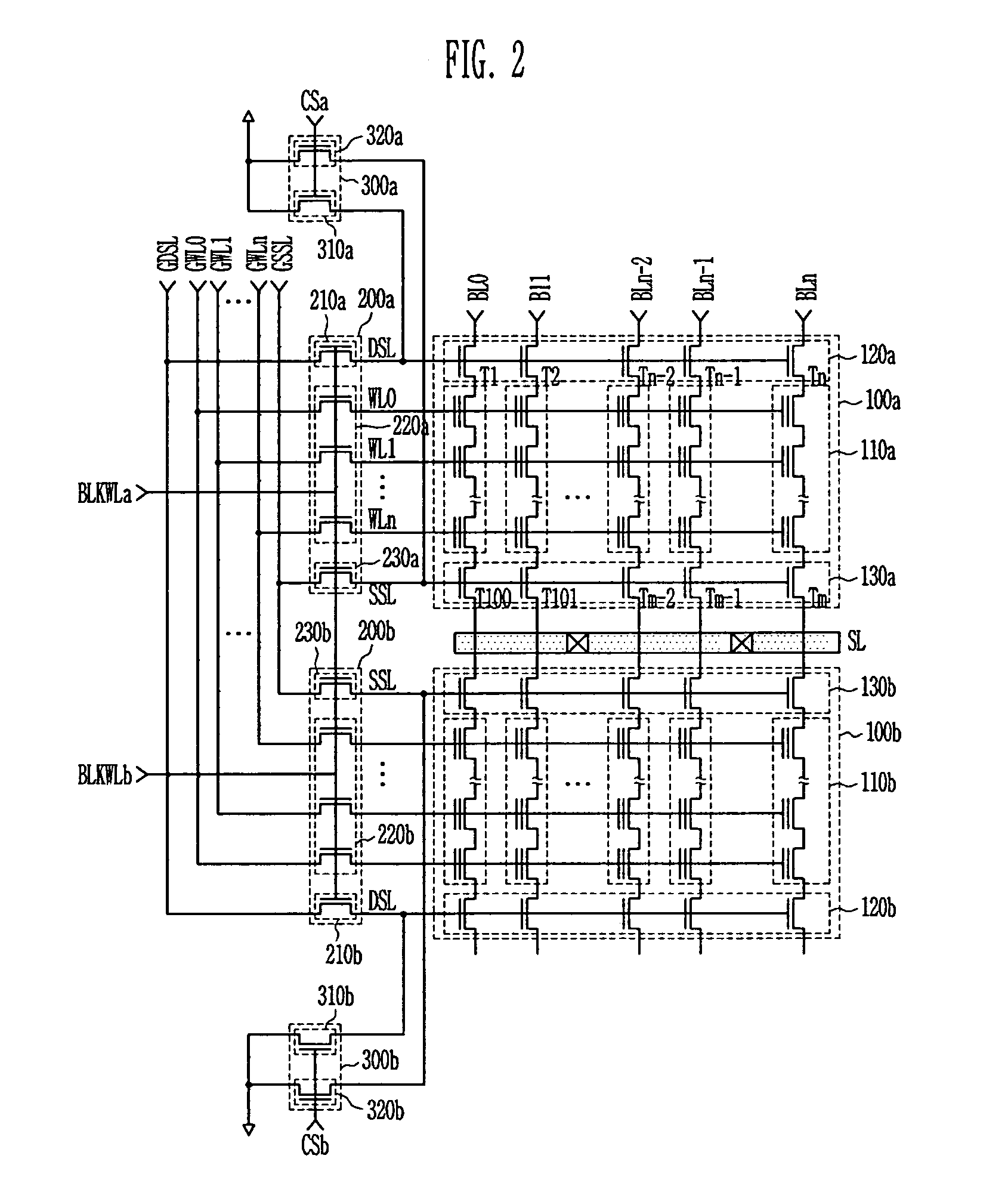
The present invention provides a NAND flash memory device and method of reading it that reduces leakage currents during a read operation. This is achieved by increasing the source-side resistance of selection transistors in the cell block. The device includes a cell block with a string selector, source selector, cell string unit, X-decoder, and switching circuit. The method involves applying global string and source selection voltages to the X-decoder, applying a pass voltage to deselected wordlines, and applying the operation voltage to the X-decoder of the selected cell block. The invention improves the speed and accuracy of NAND flash memory reading.

Problems solved by technology

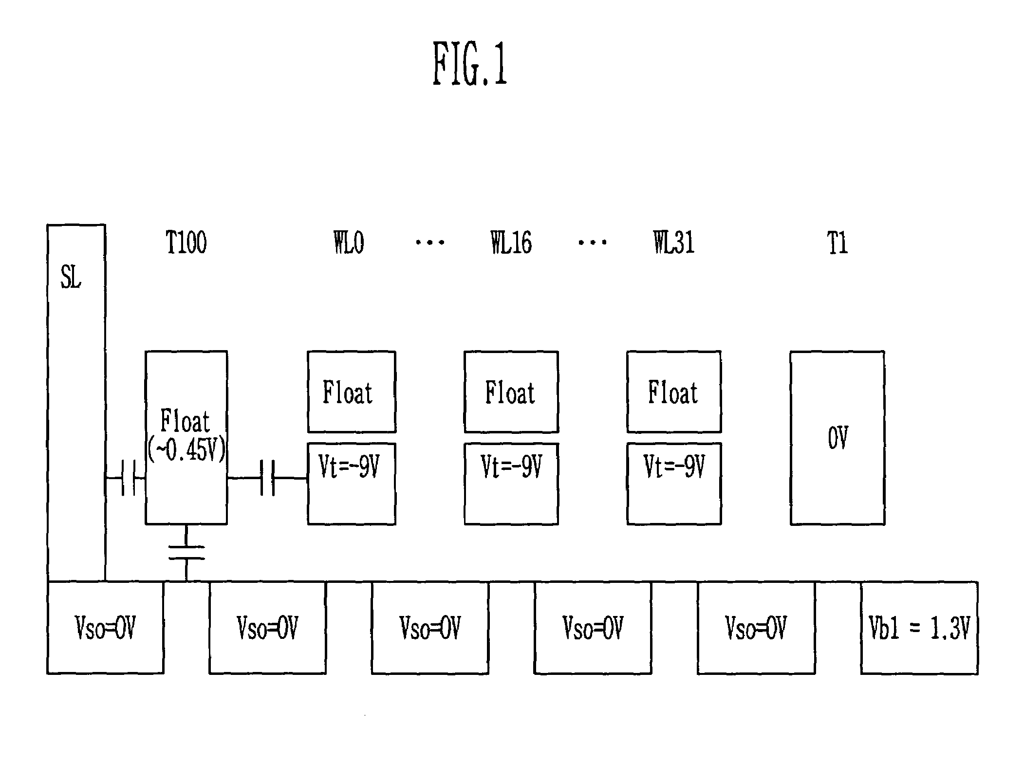
With such voltage conditions, leakage currents arising from drain selection transistors and source selection transistors may cause malfunctions in the NAND flash memory device.
Such shrinking-down in morphological configuration in the NAND flash memory device is inevitable to be weak in junction-to-junction leakage, i.e., a punch-through.

Method used


Image

  • NAND flash memory device and method of reading the same
  • NAND flash memory device and method of reading the same
  • NAND flash memory device and method of reading the same

Examples


Embodiment Construction

[0018]Preferred embodiments of the present invention will be described below in more detail with reference to the accompanying drawings. The present invention may, however, be embodied in different forms and should not be constructed as limited to the embodiments set forth herein. Rather, these embodiments are provided so that this disclosure will be thorough and complete, and will fully convey the scope of the invention to those skilled in the art. Like numerals refer to like elements throughout the specification.

[0019]In the embodiment of the present invention, a single cell block is composed of cell strings grouped with sharing wordlines, each cell string being constructed of a plurality of memory cells. Each cell string constituting the cell block is connected to a global bitline in parallel with a plural number of 1024 or 2048. And, as the cell blocks are arranged in the form of mirror image that is symmetrical on the selection transistor, a string outside junction of the selec...


PUM


Abstract

Provided is related to a NAND flash memory device and method of reading the same, in which during a read operation, a ground voltage is applied to string and ground selection transistors of deselected cell blocks so as to increase resistance of a string line to prevent leakage currents due to a back-bias effect. A reduced bitline leakage current increases an ON / OFF current ratio between programmed and erased cells to reduce a sensing time therein, which makes a read trip range so as to prevent variation of threshold voltages due to data retention and reading disturbance. Voltages can be independently applied to source selection lines by electrically isolating source selection transistors between the cell blocks. It is available to reduce the number of source discharge transistors by electrically connecting the source selection transistors between adjacent cell blocks.

Description

[0001]This application relies for priority upon Korean Patent Application No. 2004-0022677 filed on Apr. 1, 2004, the contents of which are herein incorporated by reference in their entirety.BACKGROUND[0002]1. Field of the Invention[0003]The present invention relates to a NAND flash memory device and method of reading the same, and more particularly, to a NAND flash memory device capable of reducing leakage currents therein.[0004]2. Discussion of Related Art[0005]A NAND flash memory device is comprised of memory cells serially connected between a drain selection transistor and a source selection transistor in the unit of 16 or 32 in number. A single block is defined as a group of memory cells associated with a cell string sharing the same wordline.[0006]It is general to distinguish the cell blocks into selected cell blocks and deselected cell blocks for a read operation in accordance with conditions of voltages applied to the cell blocks.[0007]First, considering voltage conditions a...

Claims


Application Information

Patent Timeline
Patent Type & Authority Patents(United States)
IPC IPC(8): G11C16/04G11C19/08G11C8/00G11C16/06G11C16/00G11C16/24G11C16/26H01L21/8247H01L27/10H01L27/115H01L29/788H01L29/792
CPCG11C16/24G11C16/0483G11C16/26
Inventor LEE, HEE YOUL
Owner STMICROELECTRONICS SRL
Learn More