
Method and apparatus for isolation in a data access arrangement using analog encoded pulse signaling

a data access arrangement and analog encoded pulse technology, applied in the field of data access arrangement (daa) circuits, can solve the problems of limiting the current available for on-hook functions to less than a few microamperes, affecting the transmission of signals across the isolation barrier, and affecting the transmission of signals

Inactive Publication Date: 2006-04-18
SILICON LAB INC
View PDF18 Cites 19 Cited by
  • Summary
  • Abstract
  • Description
  • Claims
  • Application Information

AI Technical Summary

Benefits of technology

[0019]An embodiment of a method for transferring information from a telephone line pair across an isolation barrier, according to the present invention, involves receiving an analog receive data signal from the telephone line pair, pulse-width-modulation (PWM) encoding the received analog receive data signal to a PWM encoded data signal that directly represents the received analog data signal, and driving the PWM encoded data signal across the isolation barrier. The method further recites receiving the PWM encoded data signal across the isolation barrier and decoding the received PWM encoded data signal. A further refinement of this embodiment calls for, in an on-hook state, converting the received analog receive data signal to a frequency encoded data signal and the step of pulse-width-modulation (PWM) encoding the received analog receive data signal further comprises PWM encoding the frequency encoded data signal to a PWM encoded data signal. In a still further refinement of this embodiment, the step of decoding the received PWM encoded data signal further comprises decoding the received PWM encoded signal into a digital count value. And in a yet still further refinement of this embodiment, the method further includes the step of directly processing the digital count value to perform one of ring detection, on-hook call monitoring, on-hook line voltage measurement, off-hook holding circuits, off-hook 2–4 wire hybrid, off-hook transmit and receive audio, and hook control.

Problems solved by technology

In addition, for line maintenance, to facilitate identifying line leakage, telephone devices are required by regulation (the exact requirements depending on the country) to restrict on-hook DC resistance to typically over 1 Megaohms (MΩ), which limits the current available for on-hook functions to less than a few microamperes.
Also, the line side circuit may be subject to overvoltage conditions that may arise due to lightning strike or a power line cross.
Transmitting signals across the isolation barrier is a significant challenge in the design of DAAs.
Also, the signals passed across the isolation barrier are subject to strong common mode noise signals.
However, discrete high voltage capacitors are relatively expensive devices, especially if they need to be highly matched, and, in addition, discrete component require assembly on a printed circuit board.
Larger and more expensive than standard high voltage capacitors are those designed to meet standards of European Norm EN60950 or similar electrical safety standards since they must either (1) meet structural minimum insulation thickness requirements of 0.4 mm and minimum creepage distance of 2.5 millimeters or (2) if standard capacitors are used, multiple caps must be used and placed in series, thereby increasing cost and board area.
Large capacitors, over 300 pF, are used in some approaches to provide higher current levels to directly power both hook control and circuitry active when on-hook, but these larger devices incur greater cost and size limitations.
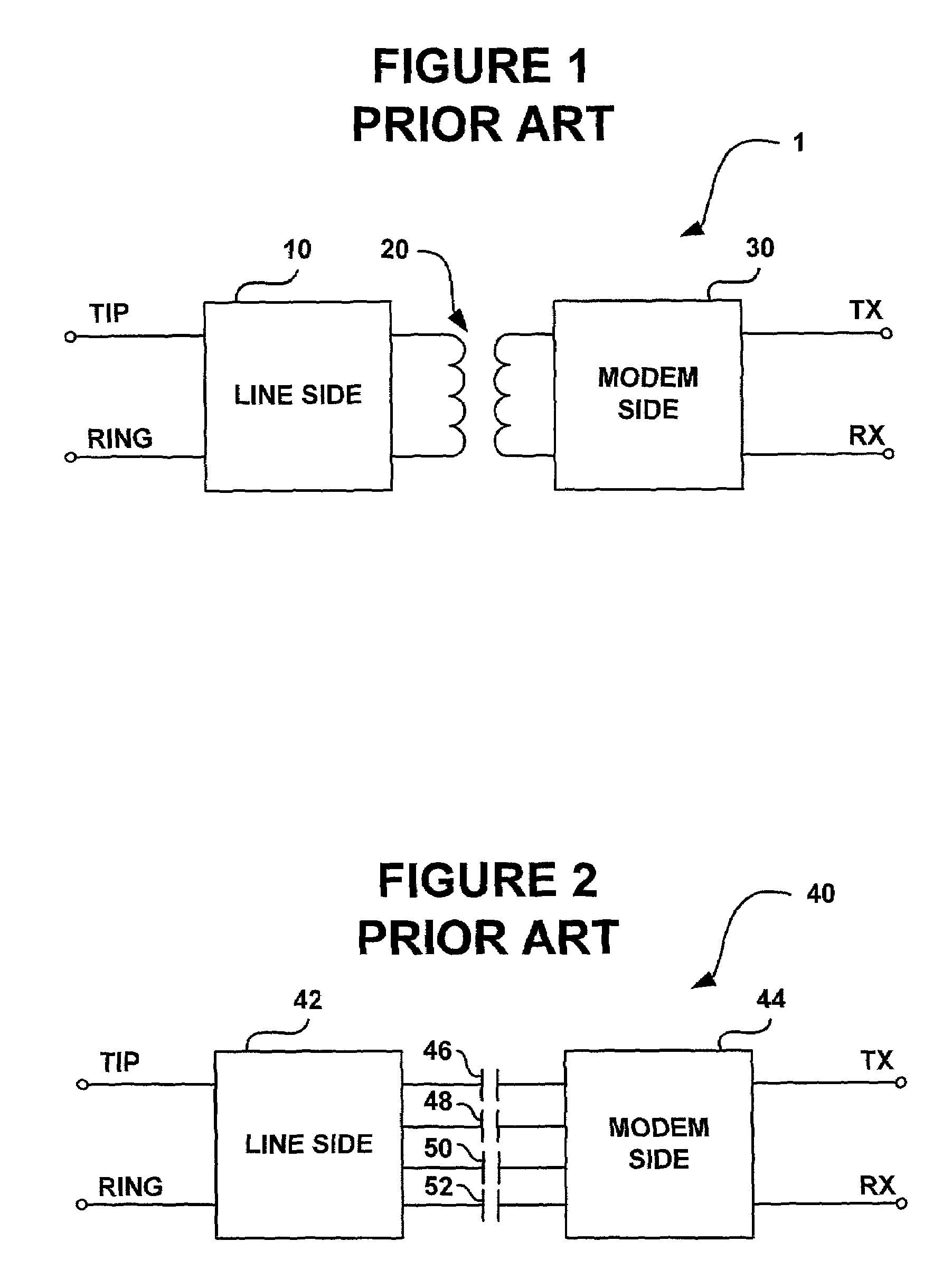
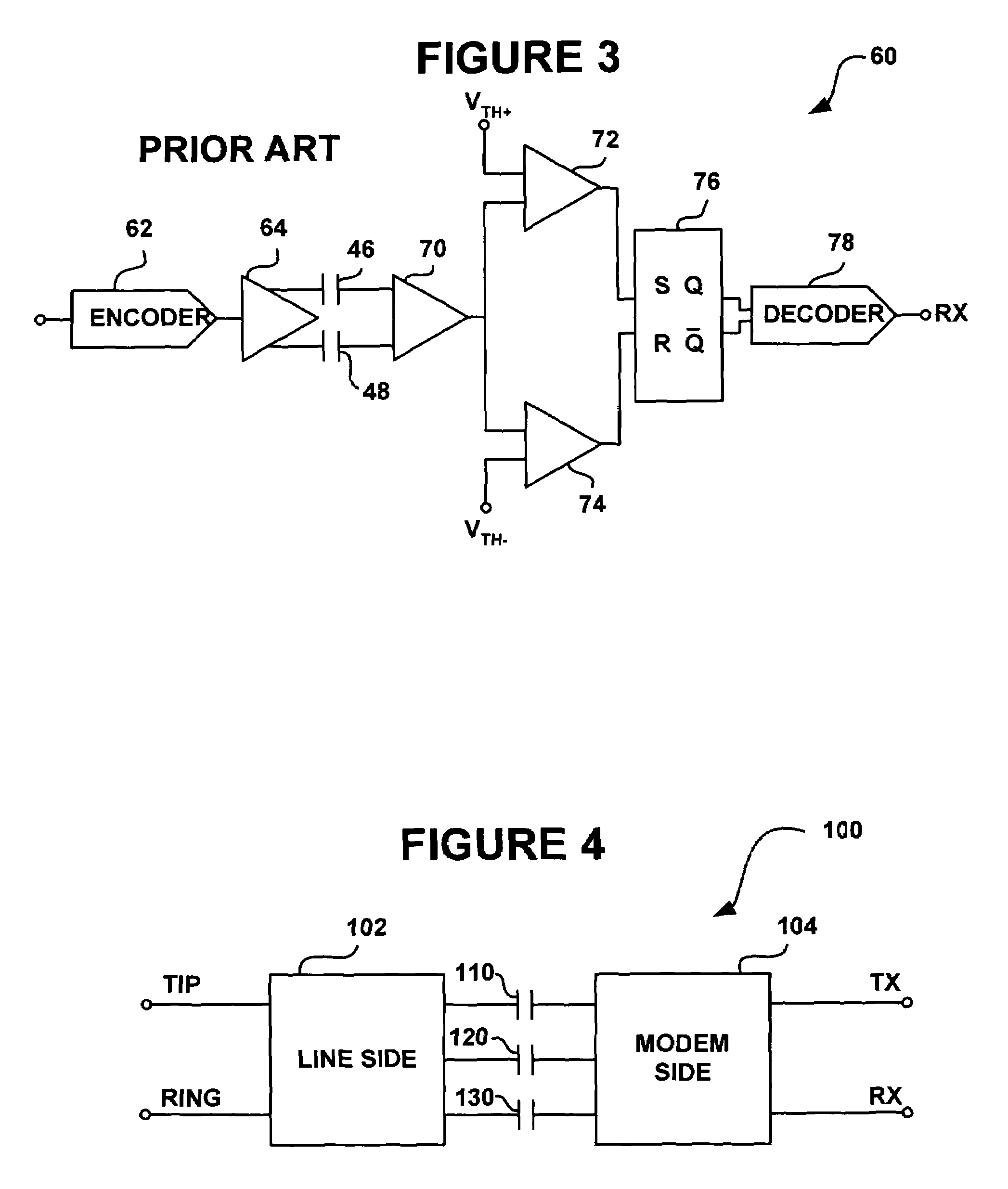
One obvious drawback is the requirement for two isolation capacitors to handle both sides of the differential signal transmitted from driver 64 to receive amplifier 70.
The market for DAAs is highly competitive and the cost required for multiple isolation capacitors per signal path can undermine the competitiveness of the resulting design.
However, AM encoding has generally poor noise immunity and is vulnerable to aliasing from radio frequency signals, most notably from AM radio broadcast stations in the 550 kHz to 1650 kHz band.
Since high speed modems need signal to noise ratios of up to 80 dB, even very low level heterodynes can impair performance.
In fact, it is this problem which requires that there be a very high level of balance on the capacitors, differential drivers, differential receivers, and board layout to minimize the effects of radio frequency interference.
Although a high speed modem DAA system typically requires a CODEC somewhere in the system, placing the CODEC on the line side adds design difficulties since the line side circuit needs both digital and complex analog circuits that must be powered from the telephone line pair.
Another issue with solid state DAAs intended for use with high speed modems is that due to the fact that the line side is typically powered from the telephone line pair and is analog in nature, this circuit is more difficult to design and often requires more revisions than the modem side IC.
Use of a fabrication process with a minimum operating voltage of 3–5V is desirable since analog designs intended for operation at or below 2.4V require specialized low voltage design techniques which are not area efficient and are also performance limited in noise, dynamic range, power, bandwidth, etc.
A BICMOS process which is cost or performance optimal for an analog design is often not cost or performance optimal for high density digital ICs.
Commonly circuits fabricated using digital CMOS processes have lower maximum operating voltages, down to as little as 1.8V, and do not have the rich assortment of analog components available on BICMOS processes.

Method used


Image

  • Method and apparatus for isolation in a data access arrangement using analog encoded pulse signaling
  • Method and apparatus for isolation in a data access arrangement using analog encoded pulse signaling
  • Method and apparatus for isolation in a data access arrangement using analog encoded pulse signaling

Examples


Embodiment Construction

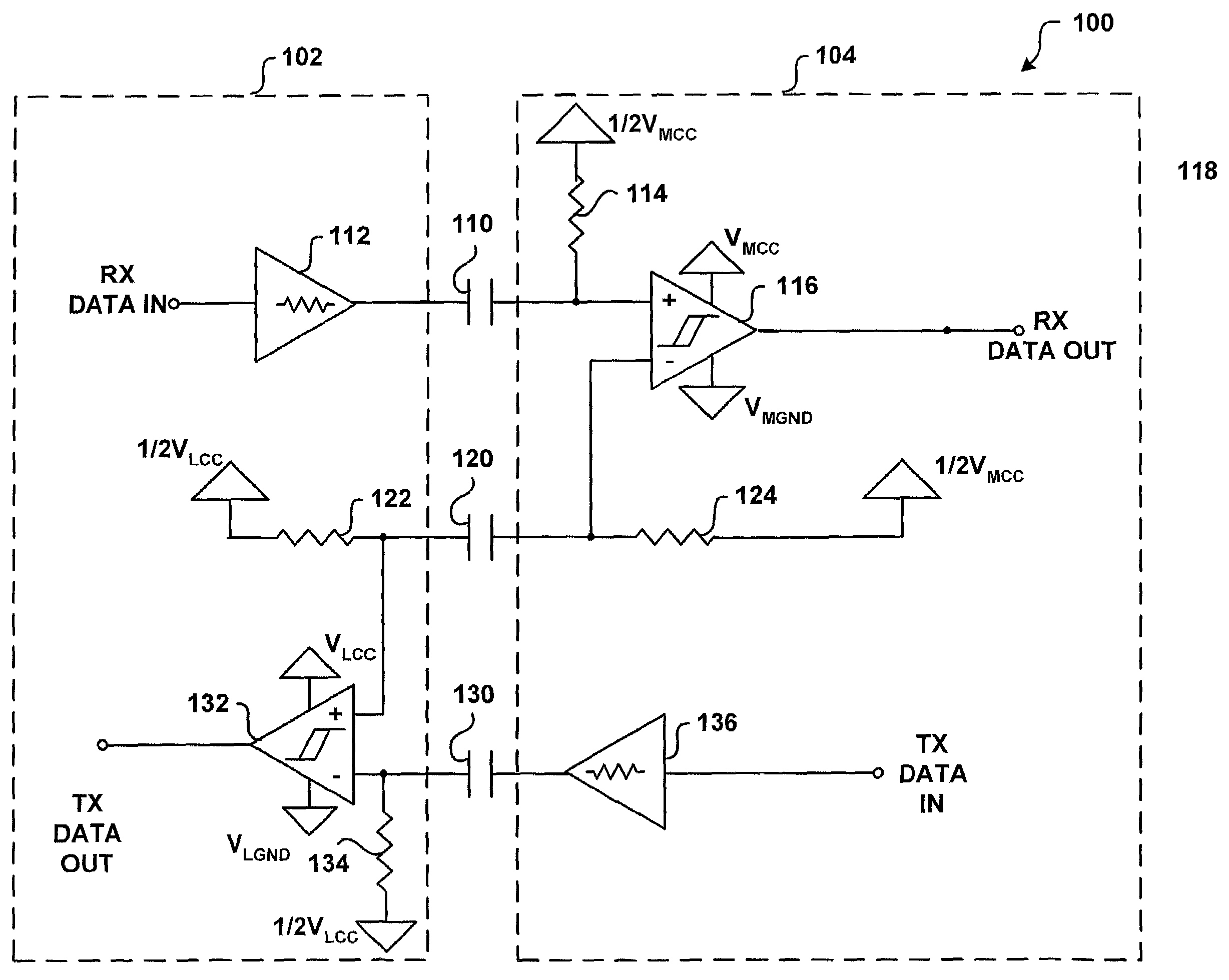
[0036]The present invention is directed toward a method and apparatus for transferring data across an isolation barrier using binary amplitude modulated pulses with fast edges. The analog information is encoded on edge timing via use of frequency modulation when on-hook and via use of pulse-width-modulation when off-hook. The binary amplitude modulated pulses are sent across capacitors with a single ended amplifier and may be received by either a single ended or differential amplifier.

[0037]Conventionally, it is well understood that converting analog signals to digital bits before sending them across a noisy communication channel (in this case the isolation capacitors) is one method to prevent incremental degradation of signals due to noise or distortion. Digital information bits may be encoded on the binary amplitude of a carrier signal or encoded on edge positions of transitions in a binary carrier signal. In order for bits to become corrupted, the noise or distortion on the commu...


PUM


Abstract

The present invention is directed toward a method and apparatus for transferring data across an isolation barrier using high speed analog encoded signals. A line side circuit interfaces with tip and ring contacts on one side of a capacitive isolation barrier that isolates the line side circuit from a modem side circuit. During an on-hook state, the line side circuit converts an analog line side voltage signal to a frequency signal and then encodes the frequency signal into a high frequency pulse-width-modulated (PWM) signal. The high frequency PWM signal is transmitted across the capacitive isolation barrier to the modem side circuit. During an off-hook state, the analog line side voltage is again encoded into a high frequency pulse-width-modulated (PWM) signal for transmission across the isolation barrier. The modem side circuit recovers the transmitted PWM signal and converts it into a digital count value that represents the amplitude of the analog voltage observed at the tip and ring. The digital count value may be directly processed by a processor on the modem side or may be converted back to an analog signal.

Description

FIELD OF THE INVENTION[0001]The present invention relates to data access arrangement (DAA) circuits. More specifically, it relates to the transmission of information across an isolation barrier in a DAA.BACKGROUND OF THE INVENTION[0002]DAAs are used to provide a dielectrically isolated interface between a telephone line pair (tip and ring pair) and a telephone device such as a modem or FAX machine. A DAA is typically divided into a line side circuit for interfacing to the tip and ring contacts and a modem side circuit for interfacing to the modem or computing equipment. FIG. 1 is a functional block diagram illustrating an example of a DAA 1 that includes a line side circuit 10 for interfacing with TIP and RING terminals and a modem side 30 for interfacing to data transmit TX and receive RX terminals. There are several functions which a DAA is generally required to perform.[0003]Typically, the line side circuit of the DAA should present a controlled AC (alternating current) impedance...

Claims


Application Information

Patent Timeline
Patent Type & Authority Patents(United States)
IPC IPC(8): H04M1/00H04M9/00H04M9/08H04B14/02H04L25/49
CPCH04B14/026H04L25/4902H04L25/0268
Inventor HOLCOMBE, WAYNE T.PARDOEN, MATTHIJS D.
Owner SILICON LAB INC
Learn More