Eureka AIR delivers breakthrough ideas for toughest innovation challenges, trusted by R&D personnel around the world.

Active block write-back from SRAM cache to DRAM

a write-back and active block technology, applied in the field of computer graphics, can solve the problems management functions, and data and data rates, and achieve the effects of increasing the difficulty and cost of integration of cache management functions and management functions

Inactive Publication Date: 2006-04-11
ORACLE INT CORP
View PDF22 Cites 16 Cited by
  • Summary
  • Abstract
  • Description
  • Claims
  • Application Information

AI Technical Summary

Benefits of technology

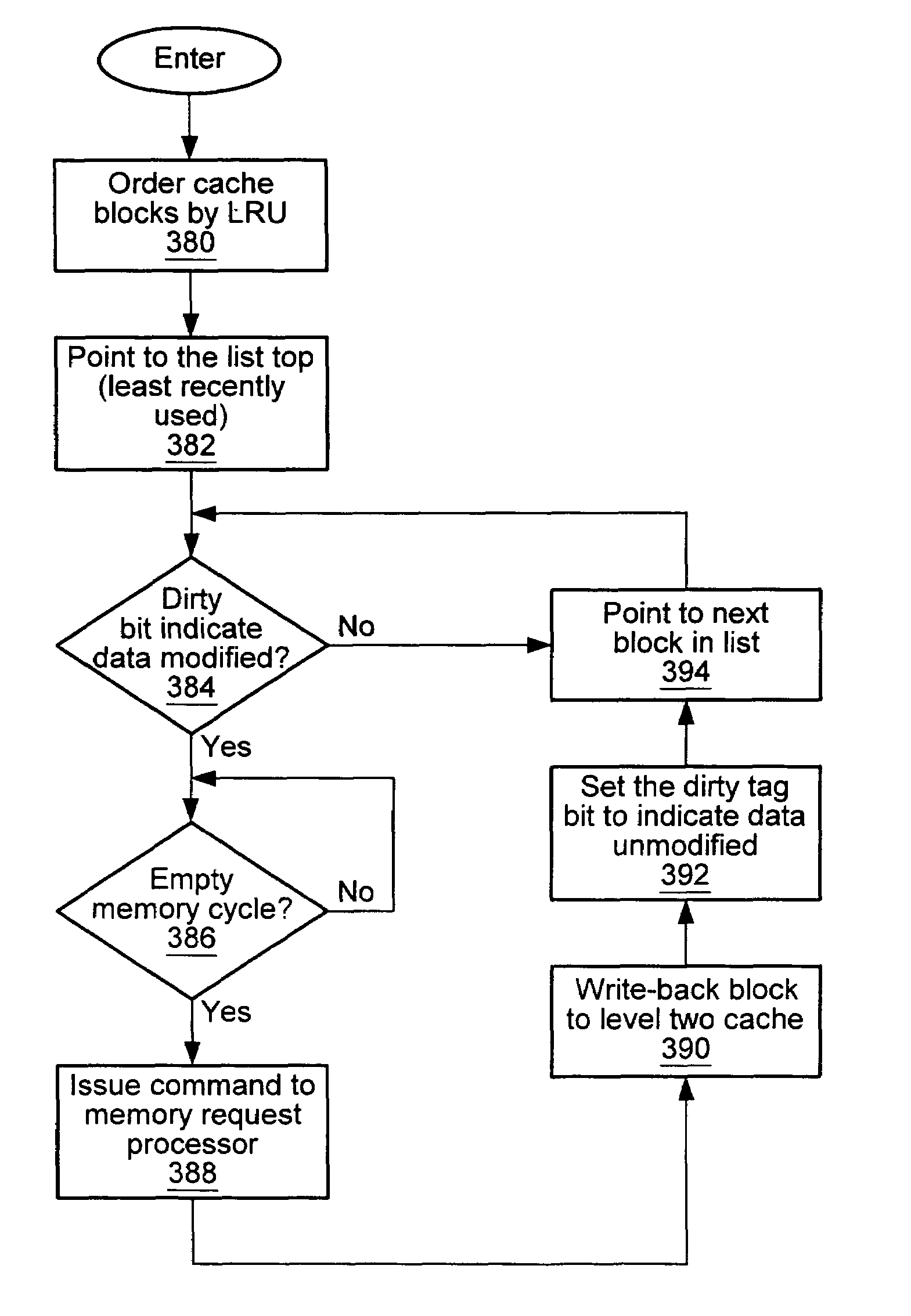
[0007]The problems set forth above may at least in part be solved in some embodiments by a system or method for managing a 3D-RAM cache through the employment of external dirty tag bits and LRU (i.e., least recently used) registers. In one embodiment, the system may include a memory array of 3D-RAM devices configured to receive and store pixel data. A memory request processor may be connected to the memory and may be configured to maintain an array of dirty tag bits (i.e., setting and clearing the logic state of the dirty tag bits in response to cache requests and pixel write operations) and a list of LRU registers. The level one cache of the 3D-RAM may be divided into logical blocks, with one dirty tag bit and one LRU register associated with each block. The memory request processor may be further configured to periodically synchronize the pixel data in the 3D-RAM level two and level one caches by commanding level one cache write-backs of blocks according to the contents of the LRU registers and dirty tag bits.
[0008]As noted above, a method for managing 3D-RAM cache through the employment of external dirty tag bits and LRU registers is also contemplated. In one embodiment, the method

Problems solved by technology

This consistent increase in data and data rates places additional burden on the memory systems that form an integral part of the graphics system.
However, as these devices have grown in capacity and performance, it has become increasingly difficult and costly to integrate these cache management functions.
In the most recent 3D-RAM device, the 3D-RAM64 these cache management functions have been abandoned altogether having finally become economically infeasible.

Method used


Image

  • Active block write-back from SRAM cache to DRAM
  • Active block write-back from SRAM cache to DRAM
  • Active block write-back from SRAM cache to DRAM

Examples


Embodiment Construction

Computer System—FIG. 1

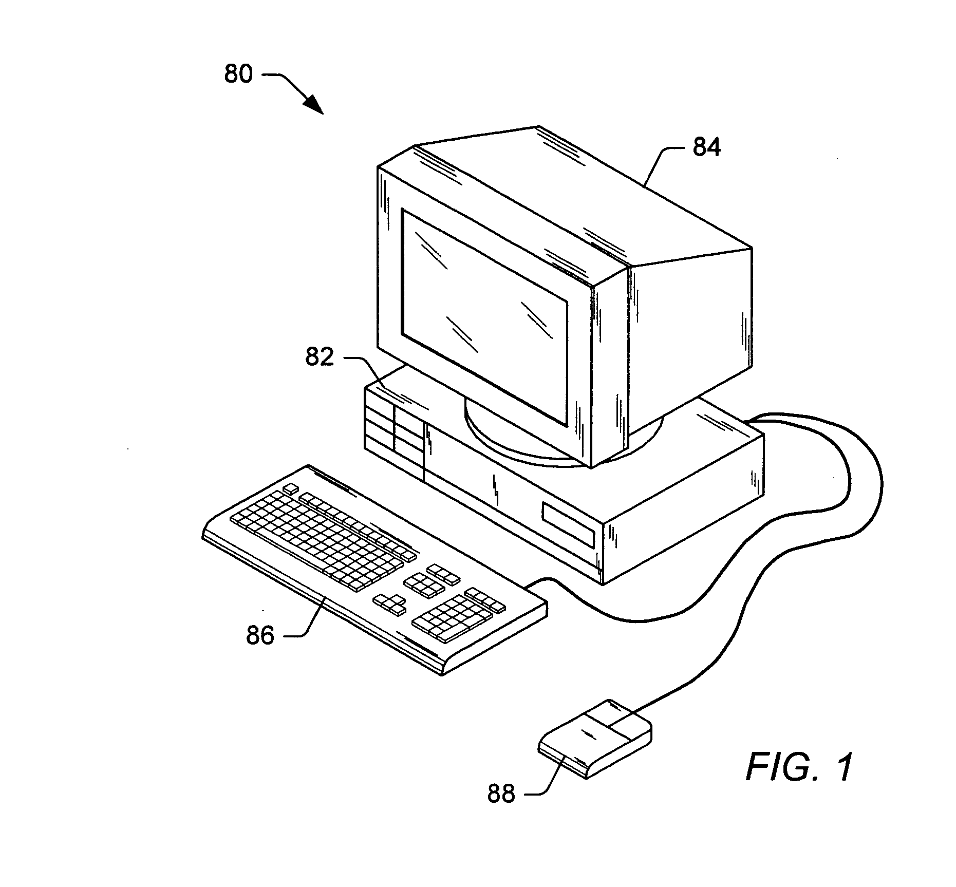
[0025]Referring now to FIG. 1, one embodiment of a computer system 80 that includes a graphics system that may be used to implement one embodiment of the invention is shown. The graphics system may be comprised in any of various systems, including a computer system, network PC, Internet appliance, a television, including HDTV systems and interactive television systems, personal digital assistants (PDAs), virtual reality systems, and other devices which display 2D and or 3D graphics, among others.

[0026]As shown, the computer system 80 comprises a system unit 82 and a video monitor or display device 84 coupled to the system unit 82. The display device 84 may be any of various types of display monitors or devices (e.g., a CRT, LCD, or gas-plasma display). Various input devices may be connected to the computer system, including a keyboard 86 and / or a mouse 88, or other input device (e.g., a trackball, digitizer, tablet, six-degree of freedom input device, head trac...


PUM


Abstract

An external cache management unit for use with 3D-RAM and suitable for use in a computer graphics system is described. The unit maintains and tracks the status of level one cache memory in the 3D-RAM. The unit identifies dirty blocks of cache memory and prioritizes block cleansing based on a least used algorithm. Periodic block cleansing during empty memory cycles is provided for, and may also be prompted on demand.

Description

BACKGROUND OF THE INVENTION[0001]1. Field of the Invention[0002]This invention relates generally to the field of computer graphics and, more particularly, to graphics frame buffer architecture.[0003]2. Description of the Related Art[0004]With each new generation of graphics system, there is more image data to process and less time in which to process it. This consistent increase in data and data rates places additional burden on the memory systems that form an integral part of the graphics system. Attempts to further improve graphics system performance are now running up against the limitations of these memory systems in general, and memory device limitations in particular.[0005]In order to provide memory systems with increased data handling rates and capacities, system architects may employ consistently higher levels of integration. One example of increased integration is the 3D-RAM family of memories from the Mitsubishi Corporation. The 3D-RAM incorporates four banks of DRAM main ...

Claims


Application Information

Patent Timeline
IPC IPC(8): G09G5/36G06F12/00G06F13/00G06T1/60G09G5/39
CPCG06T1/60G09G5/39G09G2360/121G06F2212/455G06F12/0804G06F12/0897G06F12/126
Inventor LAVELLE, MICHAEL G.KUBALSKA, EWA M.TANG, YAN YAN
Owner ORACLE INT CORP
Why Eureka
Eureka Blog
Learn More