
Method for converting a planar transistor design to a vertical double gate transistor design

a technology of planar transistors and transistors, applied in the field of integrated circuit design, can solve the problems of excessive leakage current, large layout/design changes, and undesirable characteristics of transistors

Inactive Publication Date: 2006-03-14
TAIWAN SEMICON MFG CO LTD
View PDF7 Cites 63 Cited by
  • Summary
  • Abstract
  • Description
  • Claims
  • Application Information

AI Technical Summary

Benefits of technology

Enables the conversion of existing integrated circuit designs to vertical double gate transistors with improved electrostatic coupling and reduced leakage current, while minimizing the need for extensive layout changes.

Problems solved by technology

Because there is only a single gate electrode to control the channel, the transistor may exhibit undesirable characteristics.
For example, the planar transistor may suffer from certain short channel effects, where the drain electrode has an unwanted effect on the channel resulting in excessive leakage current.
However, extensive layout / design changes may be necessary when converting a design using planar transistors to a design using vertical double gate transistors.

Method used


Image

  • Method for converting a planar transistor design to a vertical double gate transistor design
  • Method for converting a planar transistor design to a vertical double gate transistor design
  • Method for converting a planar transistor design to a vertical double gate transistor design

Examples


Embodiment Construction

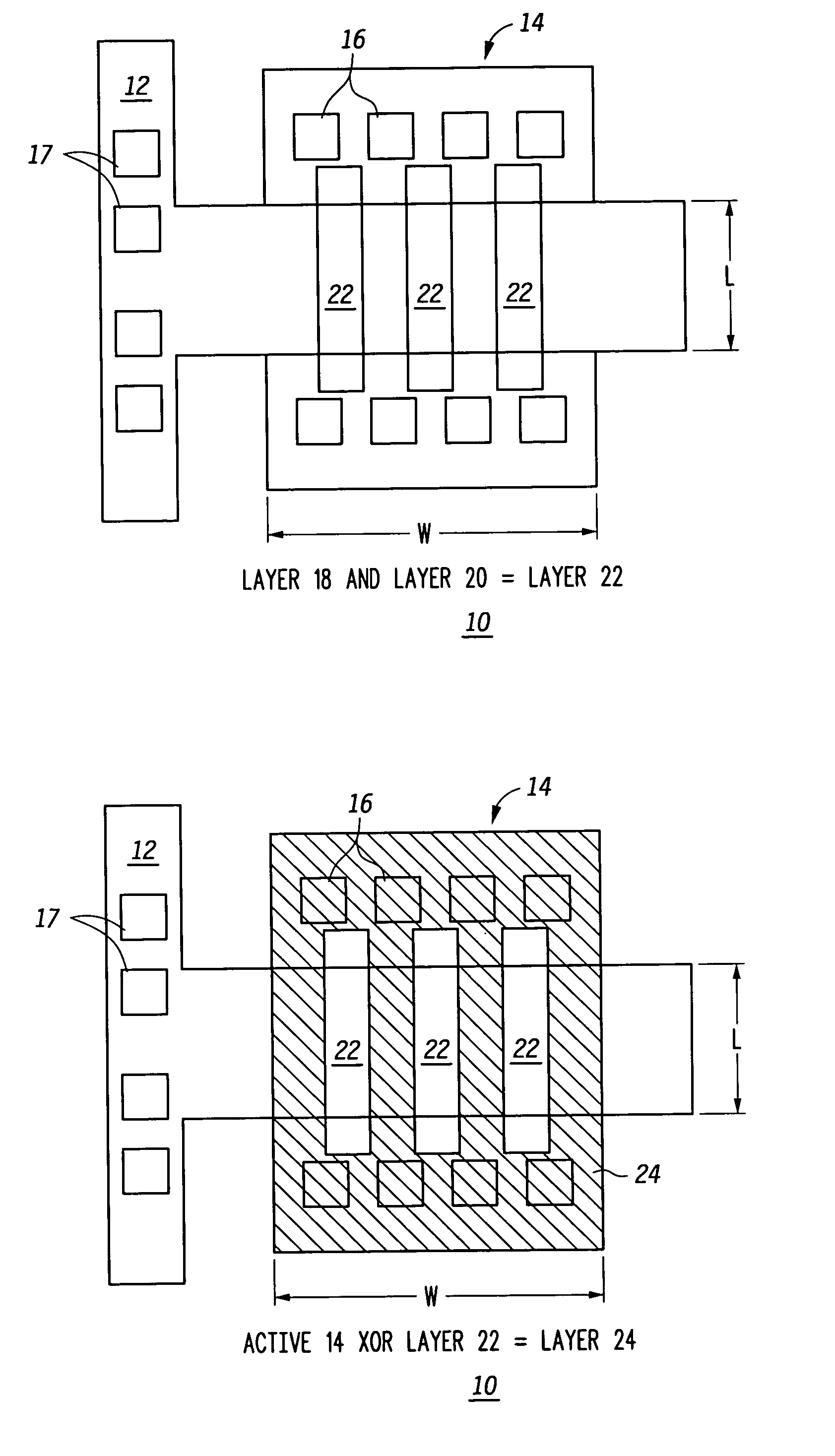
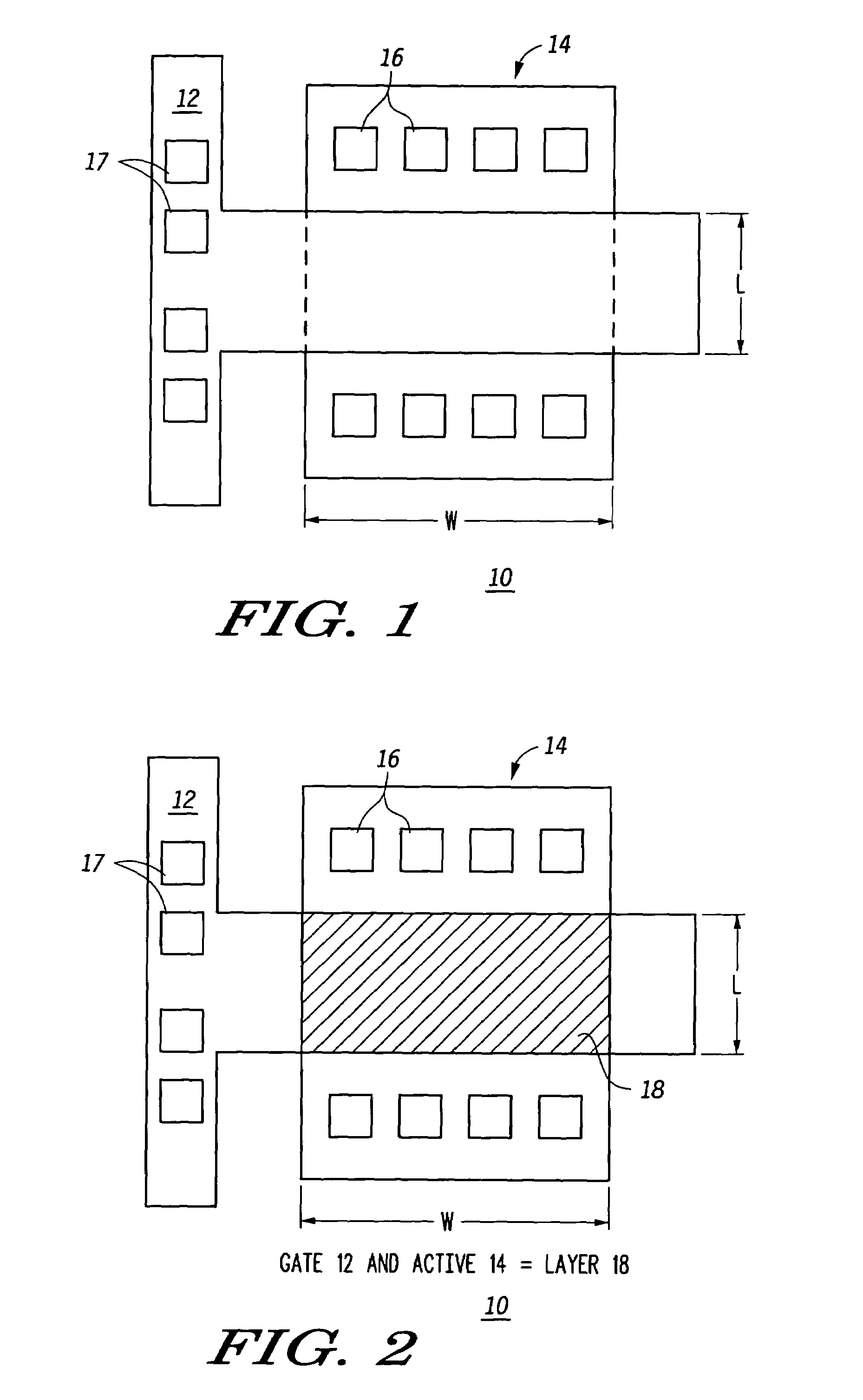
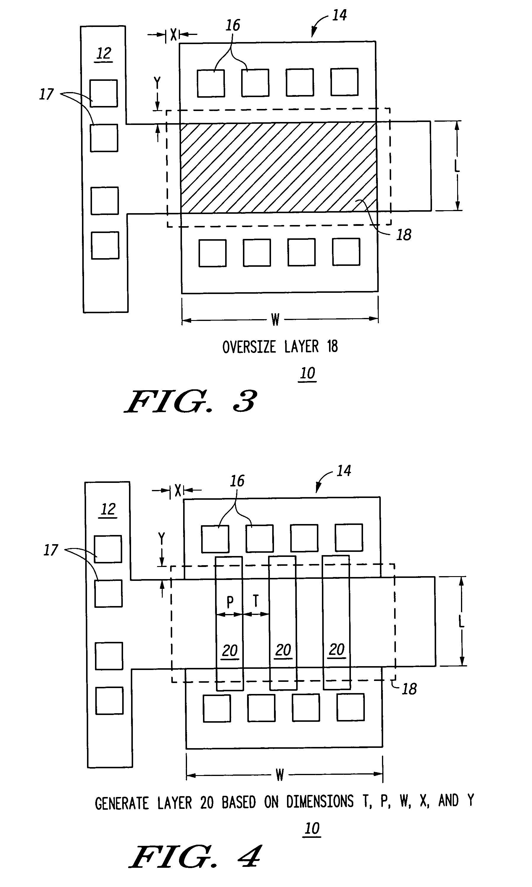
[0009]Generally, the present invention provides a method for converting a planar transistor design to a vertical double gate transistor design. The method includes providing a planar transistor layout having a gate layer overlying an active layer. In one embodiment, a first intermediate layer is defined based on an overlapping region of the gate and active layers, and, using the first intermediate layer, a second intermediate layer is created which defines a spacing between at least two fins of the vertical double gate transistor design. The second intermediate layer may also define a length L and a width of the at least two fins. One embodiment modifies a dimension of the first intermediate layer prior to defining the second intermediate layer. The method further includes defining a resulting layer based on a non-overlapping region of the second intermediate layer and the active layer. The resulting layer may then be used to create a mask and a semiconductor device corresponding to...


PUM


Abstract

A method for creating a vertical double-gate transistor design includes providing a planar transistor layout (10) having a gate layer (12) overlying an active layer (14). In one embodiment, a first intermediate layer (18) is defined based on an overlapping region of the gate and active layers, and, using the first intermediate layer, a second intermediate layer (22) is defined which defines a spacing between at least two fins of the vertical double-gate transistor design. The second intermediate layer may also define a length and a width of the at least two fins. One embodiment modifies a dimension of the first intermediate layer prior to defining the second intermediate layer. The method further includes defining a resulting layer (24) based on a non-overlapping region of the second intermediate layer and the active layer. The resulting layer may then be used to create a mask and a semiconductor device (30) corresponding to the vertical double-gate transistor design.

Description

RELATED APPLICATIONS[0001]This application is related to U.S. patent application Ser. No. 10 / 074,732, entitled “METHOD OF FORMING A VERTICAL DOUBLE GATE SEMICONDUCTOR DEVICE AND STRUCTURE THEREOF” filed Feb. 13, 2002, and assigned to the assignee hereof.FIELD OF THE INVENTION[0002]This invention relates generally to integrated circuit design, and more particularly, to a method for converting a planar transistor design to a vertical double gate transistor design.BACKGROUND OF THE INVENTION[0003]Traditionally, MOSFETs (metal oxide semiconductor field effect transistors) have been implemented with a single control electrode or gate on a planar substrate. The gate is placed between a source and drain electrode and functions to create a channel controlling the amount of current between the source and drain electrodes. Because there is only a single gate electrode to control the channel, the transistor may exhibit undesirable characteristics. For example, the planar transistor may suffer ...

Claims


Application Information

Patent Timeline
Patent Type & Authority Patents(United States)
IPC IPC(8): G06F17/50H01L21/8234H01L27/12
CPCH01L21/823437H01L29/785H01L27/1203
Inventor MATHEW, LEOMIN, BYOUNG W.
Owner TAIWAN SEMICON MFG CO LTD
Learn More