Co-planarity examination method and optical module for electronic components

a technology of optical modules and electronic components, applied in the field of machine vision, can solve the problems of inability to get separated images of electronic parts, inability to measure or handle parts causing specular reflections, and current systems have problems, so as to achieve accurate measurement of selected parts of a device, ensure the accuracy of measurement made on the part, and reduce the effect of problems

Inactive Publication Date: 2006-03-14
LEMAIRE CHARLES A
View PDF24 Cites 2 Cited by
  • Summary
  • Abstract
  • Description
  • Claims
  • Application Information

AI Technical Summary

Benefits of technology

[0011]Advantageously, the machine-vision system of the present invention can view a device under test using backlighting to minimize or substantially eliminate the problems associated with gathering useful data from images having specular reflections. The machine vision system of the present invention can accurately measure selected portions of a device under test. In addition, the machine vision system of the present invention isolates selected portions of a device under test to assure the accuracy of measurements made on the part. Yet another advantage is that one camera produces an image with all the desired views, including side views of the device under test for checking the co-planarity and a top-down view for checking that the geometry of the device under test will fit a corresponding set of pads on a circuit board. The machine vision system allows automated, high-speed, two-dimensional inspection of objects or devices under test.

Problems solved by technology

Current systems have problems.
The problems include the inability of getting separated images of portions of the electronic part.
Portions of the part causing specular reflections generally can not be measured or handled by an optical system.
In current inspection systems, backlighting has a problem since the various features to be viewed are not separated.
The result is that the information sought, such as co-planarity and other critical parameters may not be accurately obtained since the features behind a critical portion of the object or device under test can not be viewed separately.
In other words, the data collected on backlit parts may be bad since another portion of the device under test may introduce error in the measurement of the part.
U.S. Pat. No. 4,959,898 also has problems.

Method used


Image

  • Co-planarity examination method and optical module for electronic components
  • Co-planarity examination method and optical module for electronic components
  • Co-planarity examination method and optical module for electronic components

Examples


first embodiment

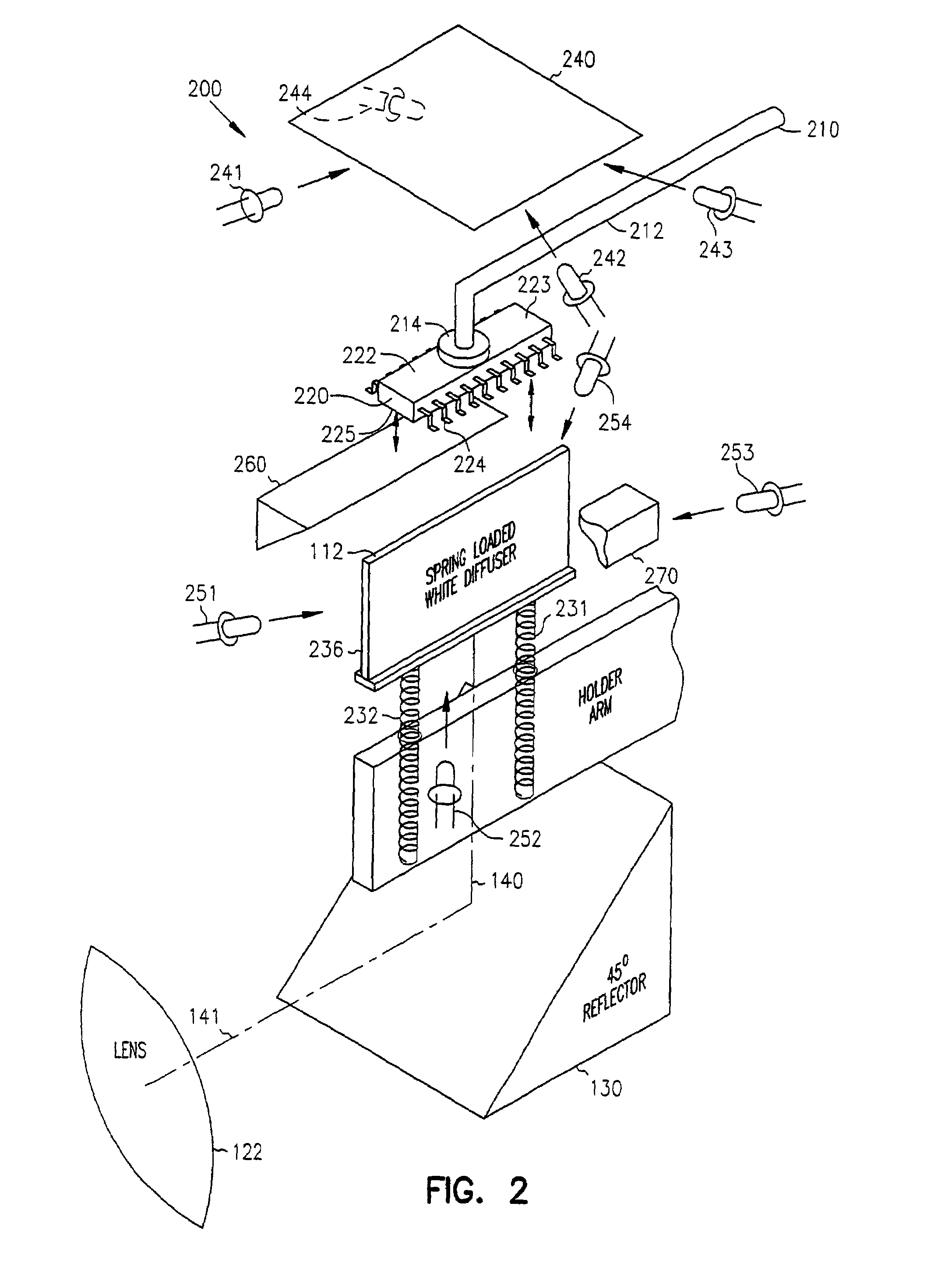
[0041]FIG. 2 is an exploded view of the present invention. FIG. 2 includes a lens 122 of the image device 120 as well as the 45° reflector or mirror 130 which converts a light path 140 from a substantially vertical orientation to a light path 141 having a substantially horizontal orientation and directed toward the lens 122 of the image device (shown in FIG. 1). The machine-vision system 200 shown in FIG. 2 includes a vacuum pick-and-place machine 210 which includes a vacuum line 212 and a vacuum pickup end 214. The vacuum pick-and-place apparatus 210 picks up objects 220 or devices under test 220 which are to be inspected. As shown in FIG. 2, the object 200 or device under test 220 is a surface-mount technology package having a substrate 222 and gull-wing type leads 224. The gull-wing shaped leads 224 are on a first side or edge and a second side or edge of the substrate 222. In other embodiments, the device under test includes solder balls affixed to the bottom surface, some of wh...

embodiment 600

[0051]FIG. 6A is a schematic view of another embodiment of the present invention 600 in which one diffuser 240 is positioned above the device under test 220. A pick-and-place assembly 210 places a part under test or device under test 220 onto a base 610. The base includes a diffuser 630 attached a portion of the base 610 which is closest to the second major surface 225 of the device under test 220. The base 610 also includes a first 45° mirrored or reflective surface 614 and a second mirrored or reflective surface 616 which is also at 45°. Light is directed at the top-down view diffuser 240 as well as at the diffuser 630. In one embodiment, the LEDs are used as light sources to back light the diffuser 630 in the top-down view diffuser 240. Also included in the machine-vision system 600 is a left-side mirror 260 and a right-side mirror 270. In addition to the left-side mirror 260, there is a first lower side mirror 660 and a second lower side mirror 662. Both of these mirrors 660, 66...

embodiment 700

[0055]In some embodiments, the L-shaped diffuser 732, 731 is backlit and can be used for both the top-down views 780, 782 and the side views 790, 792. The embodiment 700, shown in FIG. 7A, includes a base 750. The base 750 includes mirrored surfaces 614 and 616. The device under test 220 does not have to contact a portion of the base and, therefore, the base 750 does not have to be spring loaded. In some embodiments, the base may be extended to include the mirrors 662 and 672. With respect to the light paths needed to obtain all four of the images 780, 782, 790, 792, the light paths are essentially the same as those shown and described in FIG. 6A with the exception that the gull-wing leads shown are on a part that is in the dead-bug position. Each of the paths A1, A2, B1, B2 are equal in length so that the lens 122 need not accommodate different focal lengths. The light path A1 is essentially the same in FIG. 7A as in FIG. 7B and the light path B1 is essentially the same in FIG. 7A ...


PUM

PropertyMeasurementUnit
anglesaaaaaaaaaa
anglesaaaaaaaaaa
elastomericaaaaaaaaaa

Abstract

Manufacturing lines include inspection systems for monitoring the quality of parts produced. Manufacturing lines for making semiconductor devices generally inspect each fabricated part. The information obtained is used to fix manufacturing problems in the semiconductor fab plant. A machine-vision system for imaging an object having a first side and a second side includes an imager, and an optics apparatus that images two or more views of the first side of the object and images two or more views of the second side of the object. The two or more views of the first side and the second side of the object are each from different angles. The object includes at least one major surface. A divider background surface is placed near the at least one major surface of the object to obtain separate images of features of the object on the first side of the object and features of the object on the second side of the object. In one embodiment, the divider diffuses light to back light the features on the object on the first side and back light the features on the second side of the object.

Description

CROSS-REFERENCES TO RELATED INVENTIONS[0001]This is a continuation of prior U.S. patent application Ser. No. 10 / 099,684 entitled “CO-PLANARITY AND TOP-DOWN EXAMINATION METHOD AND OPTICAL MODULE FOR ELECTRONIC LEADED COMPONENTS,” filed Mar. 15, 2002 now U.S. Pat. No. 6,813,016, which is hereby incorporated in its entirety by reference,FIELD OF THE INVENTION[0002]This invention relates to the field of machine vision, and more specifically to a mechanical apparatus and method for obtaining inspection data for parts in a manufacturing environment. More particularly, the present invention relates to obtaining inspection data for two sides, edges, or surfaces of a part and displaying the same on an imaging device.BACKGROUND OF THE INVENTION[0003]There is a widespread need for inspection data for electronic parts in a manufacturing environment. One common inspection method uses a video camera to acquire two-dimensional images of a device-under-test. Current systems have problems. The probl...

Claims


Application Information

Patent Timeline
Patent Type & Authority Patents(United States)
IPC IPC(8): G01N21/00G01N21/956
CPCG01N21/8806G01N21/95684G01N2021/8812G01N2021/95661G01N2021/8832G01N2021/8887G01N2021/8816
Inventor QUIST, BRADLEY L.
Owner LEMAIRE CHARLES A
Why Eureka
Try Eureka