
Versatile system for controlling semiconductor topography

a semiconductor topography and reverse technology, applied in semiconductor/solid-state device testing/measurement, instruments, computing, etc., can solve the problems of affecting the process yield, the circuit generates numerous challenges to the semiconductor manufacturing process, and the copper is very difficult to etch in the majority of the semiconductor process flow, so as to achieve easy, efficient and cost-effective

Active Publication Date: 2006-03-07
TEXAS INSTR INC
View PDF4 Cites 4 Cited by
  • Summary
  • Abstract
  • Description
  • Claims
  • Application Information

AI Technical Summary

Benefits of technology

[0010]The present invention provides a versatile system for controlling the post-processing topology of a semiconductor wafer in an easy, efficient and cost-effective manner. The present invention is particularly applicable to controlling the post-CMP topology of a semiconductor wafer. The present invention provides direct control of CMP processing, responsive—in a dynamic or quasi-dynamic fashion—to a comprehensive profilometry evaluation.
[0011]The present invention provides a system that is readily integratable with high-volume semiconductor manufacturing processes. The system of the present invention does not require additional device processing steps but, rather, provides modeling and control subsystems that direct CMP processes in a desired manner. The modeling and control subsystems of the present invention cooperate with a profilometry evaluation system—one that provides accurate and timely data regarding current post-CMP topology—to determine the CMP modifications necessary to effect a desired post-CMP topology. The present invention thus optimizes CMP processing to provide desired post-CMP topologies in an efficient and effective manner, overcoming certain limitations commonly associated with most conventional systems.
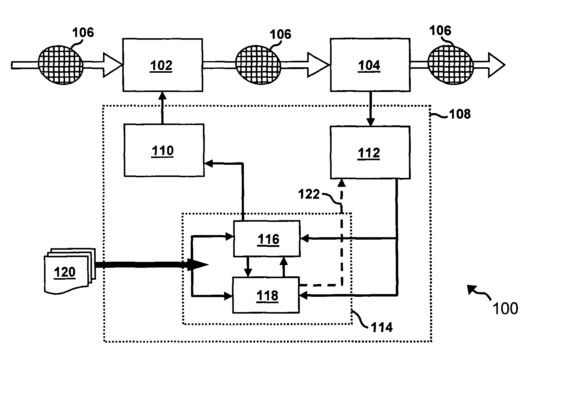
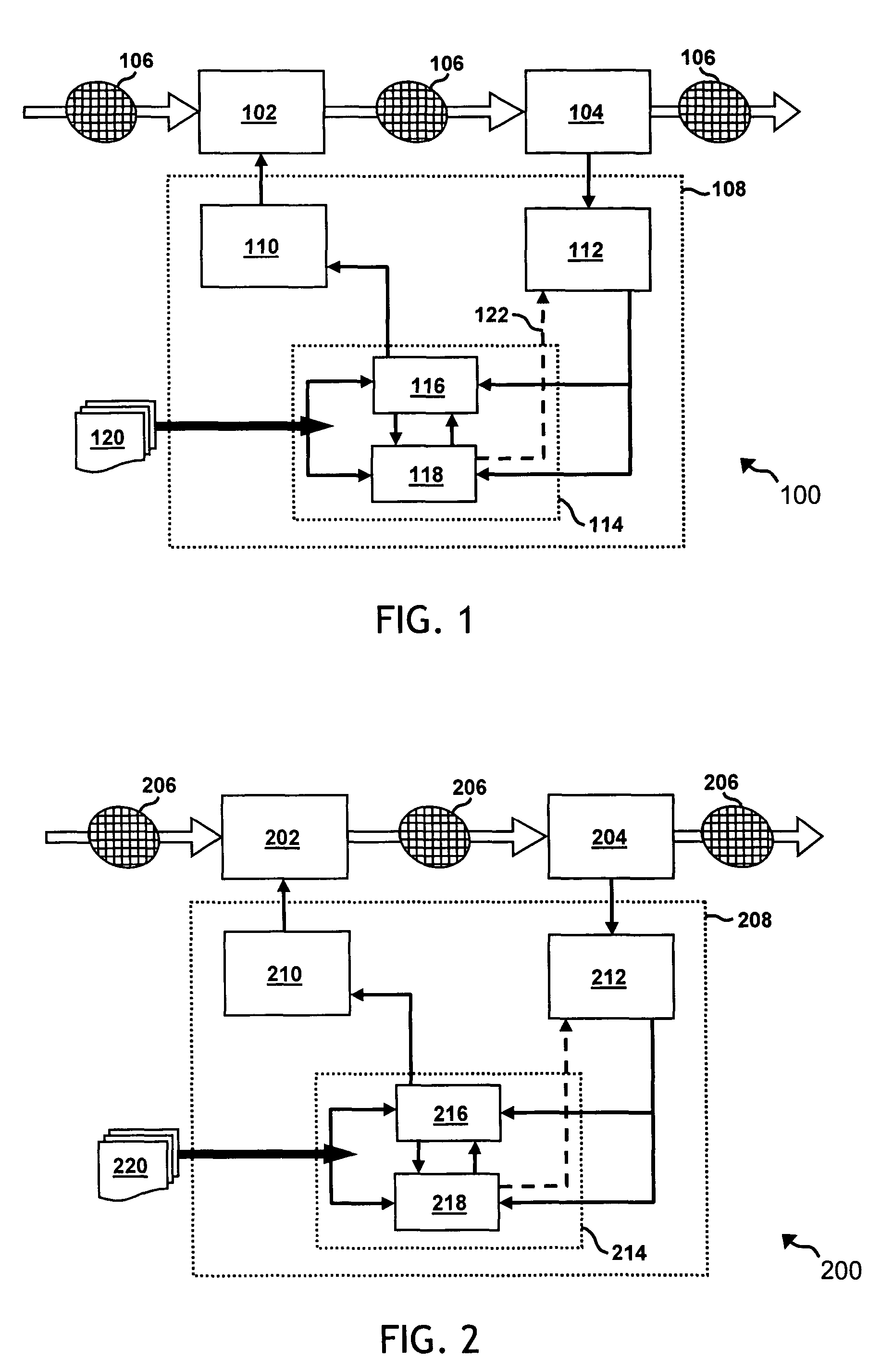
[0012]More specifically, the present invention provides a system for controlling post-CMP topology of semiconductor wafers, comprising a CMP processing function that performs CMP on a semiconductor wafer. A profilometry function renders a characterization of the actual surface topology of the semiconductor wafer after CMP. An input data set indicates a number of process variables and data points, including desired post-CMP topology for the semiconductor wafer. A control system receives the input data set and the characterization. The control system identifies any differential between the actual surface topology and the desired post-CMP topology, and eliminate that differential by altering the processing performed by the CMP processing function.

Problems solved by technology

The increased packing density of the integrated circuit generates numerous challenges to the semiconductor manufacturing process.
Unfortunately, copper is very difficult to etch in most semiconductor process flows.
Theoretically, the goal of the CMP process is to achieve a flat post-CMP topography, as excessive dishing can negatively impact process yields.
Unfortunately, a number of such conventional methods are destructive in nature, or are limited in scope to very small test areas on a wafer.
As such, these approaches are not of much use for high-volume, in-process applications.
Unfortunately, however, current profilometry approaches provide only the ability to render a relative physical measurement or characterization of post-CMP topography.
They do not provide the ability to actively control the CMP process based on metrology data.
Unfortunately, there are certain drawbacks associated with each.
Most conventional methods either require additional processing steps or changes to device layout and design—adding costs to and reducing the efficiency of production processes.
Additionally, many such conventional methods tend to be rather static in nature.
Dynamic modification of CMP on a wafer-to-wafer, or even lot-to-lot, basis in order to address subtle variations in metrology data is simply not possible or not operationally feasible.
The substantial effort and cost associated with modifying the CMP process often translates into substantial yield losses to dishing before a change can be justified.
Furthermore, many such approaches are not designed for concurrent, cooperative use with comprehensive profilometry systems and methods.

Method used


Image

  • Versatile system for controlling semiconductor topography
  • Versatile system for controlling semiconductor topography
  • Versatile system for controlling semiconductor topography

Examples


Embodiment Construction

[0021]While the making and using of various embodiments of the present invention are discussed in detail below, it should be appreciated that the present invention provides many applicable inventive concepts, which can be embodied in a wide variety of specific contexts. The invention will now be described in conjunction with providing a system for controlling CMP processing during the manufacture of semiconductor devices utilizing copper interconnects and vias. The specific embodiments discussed herein are, however, merely illustrative of specific ways to make and use the invention and do not limit the scope of the invention.

[0022]The present invention provides a versatile system for controlling the post-processing topology of a semiconductor wafer—particularly the post-CMP topology of a semiconductor wafer. The present invention provides direct control of a CMP process, responsive to a comprehensive profilometry evaluation system. Depending upon the sophistication of the manufactur...


PUM


Abstract

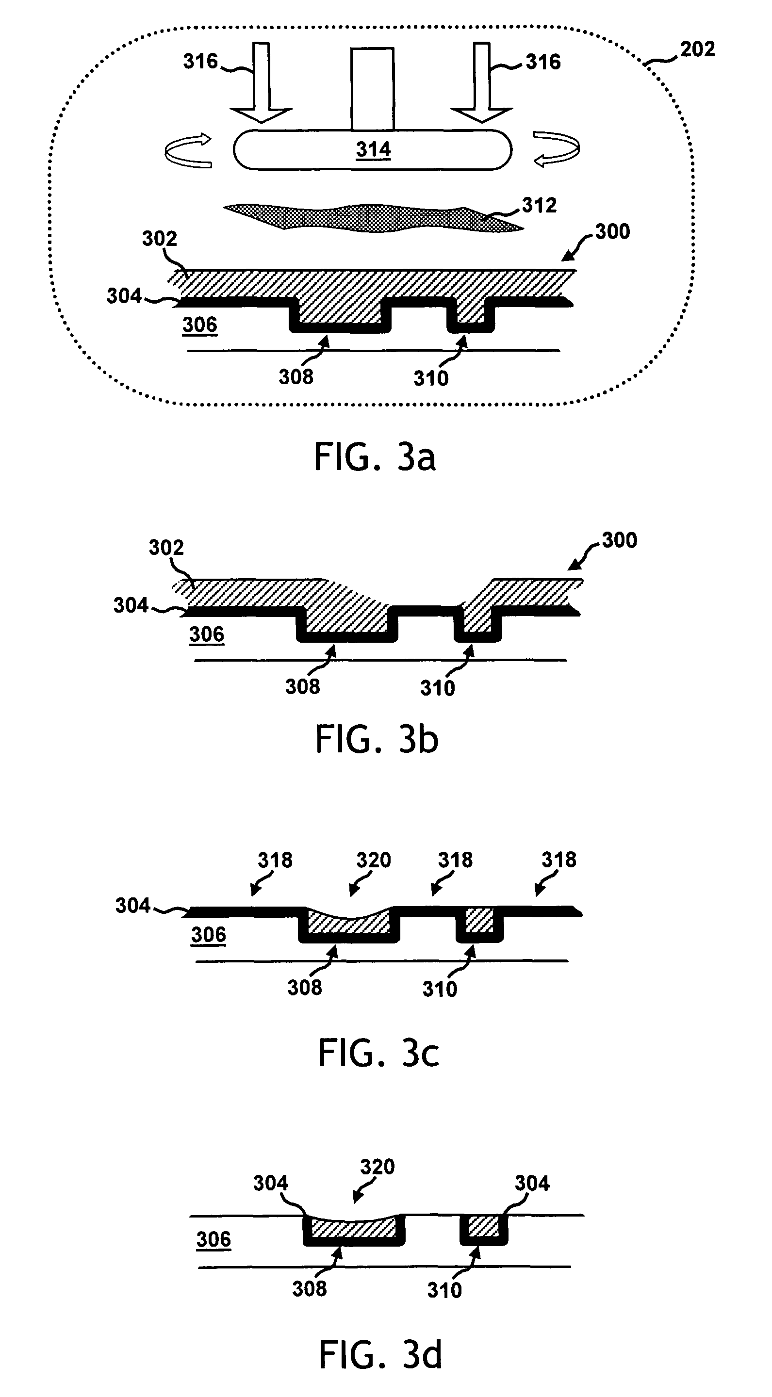
The present invention defines a system (200) for selectively controlling post-CMP dishing effects occurring in semiconductor wafers having copper metallization. The system has a CMP system (202) that performs copper overpolish and barrier polish on a copper-based semiconductor wafer (206). A profilometer (204) measures actual dishing occurring in the copper metallization after polishing. An input data set (220) includes a dishing target for the semiconductor wafer. A data integrity function (212) evaluates the profilometer's measurement, and generates an indicator of the reliability of the measurement. A modeling function (214) receives the measurement, the indicator, and the dishing target, and evaluates any differential between the dishing target and actual dishing. The modeling function generates a processing target to eliminate the differential, and modifies this process responsive to the indicator. A processing control function (210) receives the processing target, and alters the copper overpolish or barrier polish responsive to the processing target.

Description

TECHNICAL FIELD OF THE INVENTION[0001]The present invention relates generally to the field of semiconductor manufacturing processes and, more particularly, to apparatus and methods for controlling processing to effect a desired post-processing topography.BACKGROUND OF THE INVENTION[0002]The continual demand for enhanced integrated circuit performance has resulted in, among other things, a dramatic reduction of semiconductor device geometries, and continual efforts to optimize the performance of every substructure within any semiconductor device. A number of improvements and innovations in fabrication processes, material composition, and layout of the active circuit levels of a semiconductor device have resulted in very high-density circuit designs. Increasingly dense circuit design has not only improved a number of performance characteristics, it has also increased the importance of, and attention to, semiconductor material properties and behaviors.[0003]The increased packing densit...

Claims


Application Information

Patent Timeline
Patent Type & Authority Patents(United States)
IPC IPC(8): G06F19/00H01L21/00H01L21/66
CPCH01L22/20H01L21/67253
Inventor PATEL, NITAL S.TIWARI, RAJESH
Owner TEXAS INSTR INC
Learn More