System for and method of clock cycle-time analysis using mode-slicing mechanism

a clock cycle and mode-slicing technology, applied in the direction of program control, generating/distributing signals, instruments, etc., can solve the problems of over-estimating the maximum circuit delay, inability to handle combinational loops, and inability to guarantee the input stimuli that have not been simulated

Active Publication Date: 2006-02-14
SAMSUNG ELECTRONICS CO LTD
View PDF24 Cites 9 Cited by
  • Summary
  • Abstract
  • Description
  • Claims
  • Application Information

AI Technical Summary

Problems solved by technology

The disadvantage of timing simulation is that the verification cannot be guaranteed for the input stimuli that have not been simulated.
Unfortunately, there are two drawbacks with PERT: (1) it over-estimates the maximum circuit delay because it does not account for false paths, and (2) it cannot handle combinational loops that may be present in the circuit.
These algorithms are able to determine the maximum circuit delay with greater accuracy, however, they have super-linear run-time complexity (i.e., their run-time scales worse than linearly with respect to circuit size), so they are l...

Method used


Image

  • System for and method of clock cycle-time analysis using mode-slicing mechanism
  • System for and method of clock cycle-time analysis using mode-slicing mechanism
  • System for and method of clock cycle-time analysis using mode-slicing mechanism

Examples


Embodiment Construction

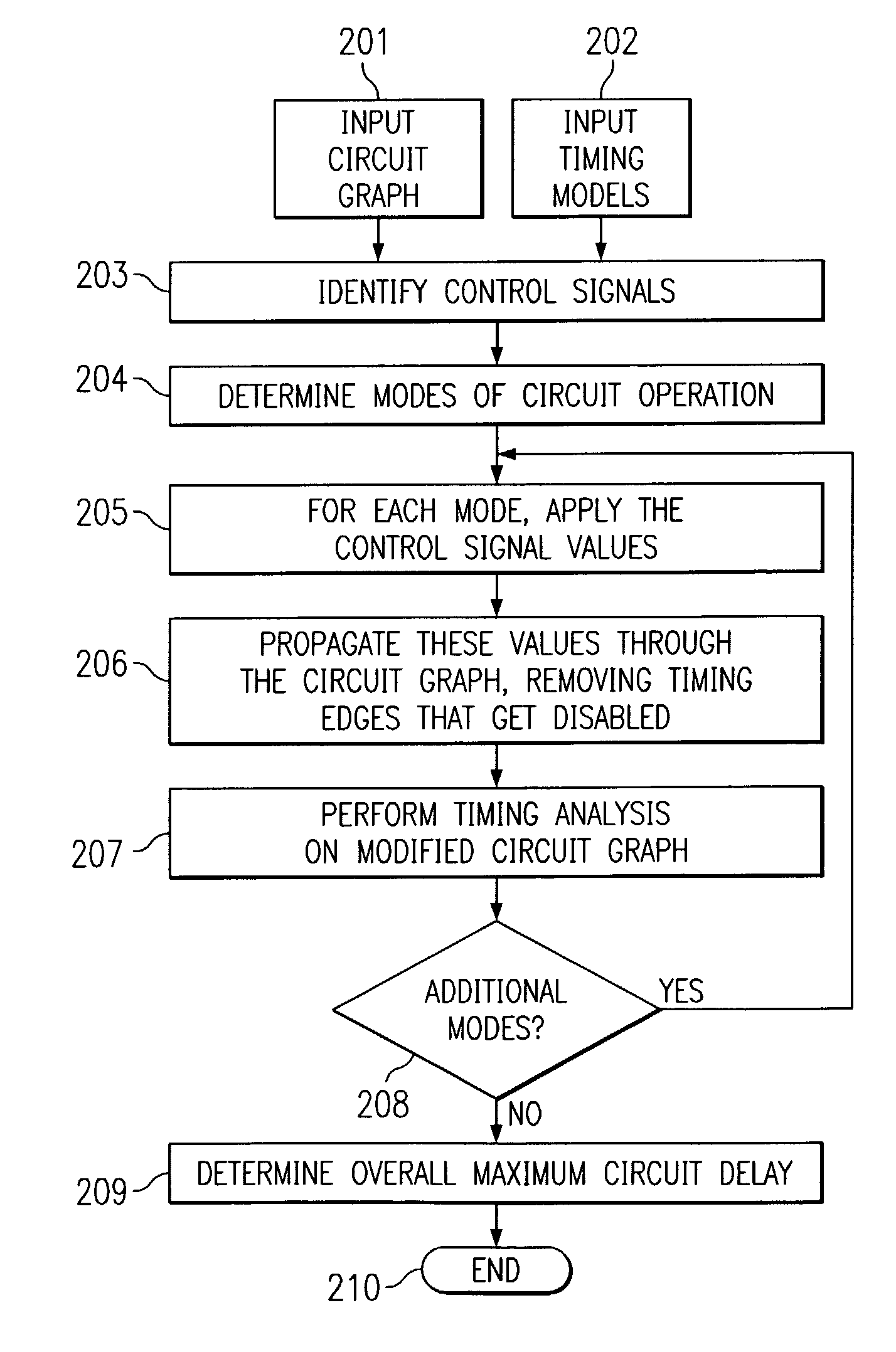
[0021]FIG. 2 is a flow diagram of an embodiment of the present invention for performing timing analysis of a digital circuit by a mode-sliced method. The flow diagram of FIG. 2 shows the provision of two inputs associated with respective input steps: input circuit graph step 201, and timing models input step 202. Input circuit graph step 201 includes providing descriptions of circuit components and the interconnections between the components of the digital circuit. A component is considered to be a hardware element that performs a set of one or more functions or operations. Muliplexers, registers, AND gates, adders, and subtractors are examples of components. The functionality of the component is also received in step 201. Interconnections refers to wires or other signal conductors that are capable of transporting data values (or signal values) in the form of electrical signals, from one point to a second point.

[0022]In step 202 timing models are received. Timing models are received...


PUM


Abstract

A method for performing a global timing analysis of a proposed digital circuit comprising receiving timing models and the proposed digital circuit; determining at least one mode of circuit operation of the proposed digital circuit; deriving a sub-circuit corresponding to each of at least one mode of circuit operation; performing timing analysis on each of the sub-circuits derived corresponding to each of the modes; and combining the timing analysis results for all of the modes to determine an overall maximum circuit delay.

Description

CROSS-REFERENCE TO RELATED APPLICATIONS[0001]The present application is related to commonly-assigned U.S. patent application Ser. No. 10 / 266,831 entitled “METHOD FOR DESIGNING MINIMAL COST, TIMING CORRECT HARDWARE DURING CIRCUIT SYNTHESIS,” and U.S. patent application Ser. No. 10 / 266,826 entitled “METHOD OF USING CLOCK CYCLE-TIME IN DETERMINING LOOP SCHEDULES DURING CIRCUIT DESIGN,” filed concurrently herewith, the disclosures of which are hereby incorporated by reference in their entireties.FIELD OF THE INVENTION[0002]The present invention is directed to digital circuit verification and, in particular, to timing analysis of digital circuits.BACKGROUND[0003]Continuing advances in technology combined with dropping production costs have led to a proliferation of electronic devices that incorporate or use advanced digital circuits including desktop computers, laptop computers, hand-held devices, such as Personal Digital Assistants (PDA), and hand-held computers, cellular telephones, pr...

Claims


Application Information

Patent Timeline
IPC IPC(8): G06F1/04G06F9/45G06F17/50
CPCG06F17/5031G06F30/3312
Inventor SIVARAMAN, MUKUNDGUPTA, SHAIL ADITYA
Owner SAMSUNG ELECTRONICS CO LTD
Why Eureka
Try Eureka