Eureka AIR delivers breakthrough ideas for toughest innovation challenges, trusted by R&D personnel around the world.

Signal balancing between voltage domains

a voltage domain and signal balancing technology, applied in the field of signal balancing, can solve problems such as the need to isolate noisy circuitry

Inactive Publication Date: 2006-01-10
MARVELL ASIA PTE LTD
View PDF17 Cites 6 Cited by
  • Summary
  • Abstract
  • Description
  • Claims
  • Application Information

AI Technical Summary

Benefits of technology

[0009]This invention is a method and media to balance signals operating on multiple power rails and thus multiple voltage conditions. Additionally it provides methods of modeling the resulting signal skew.

Problems solved by technology

Some of these islands operate at different voltages from one another, others have the ability to switch to standby or sleep mode, while still others result from the need to isolate noisy circuitry.

Method used


Image

  • Signal balancing between voltage domains
  • Signal balancing between voltage domains
  • Signal balancing between voltage domains

Examples


Embodiment Construction

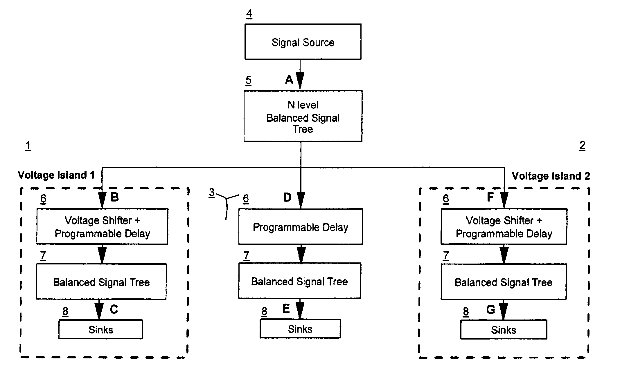
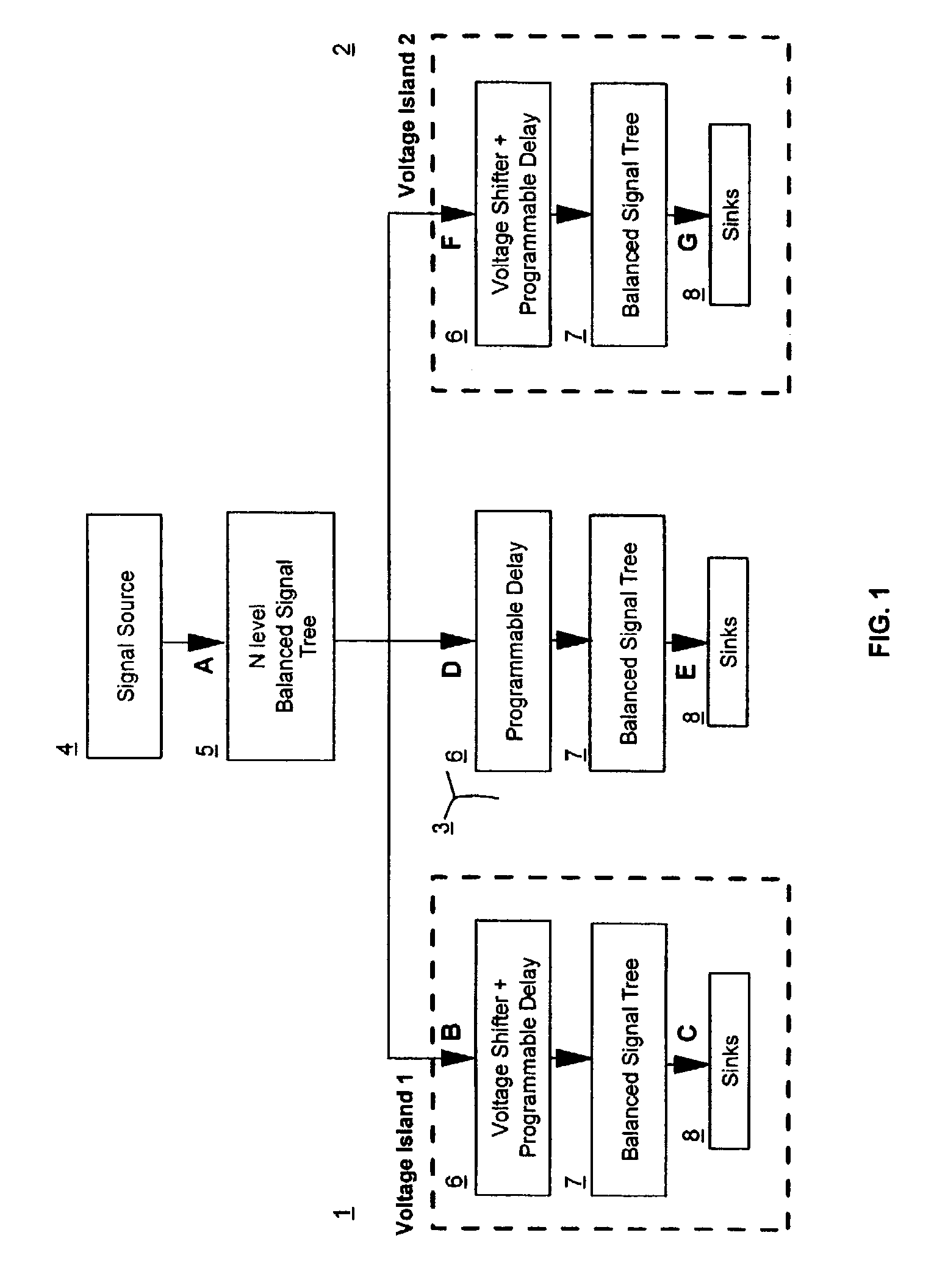
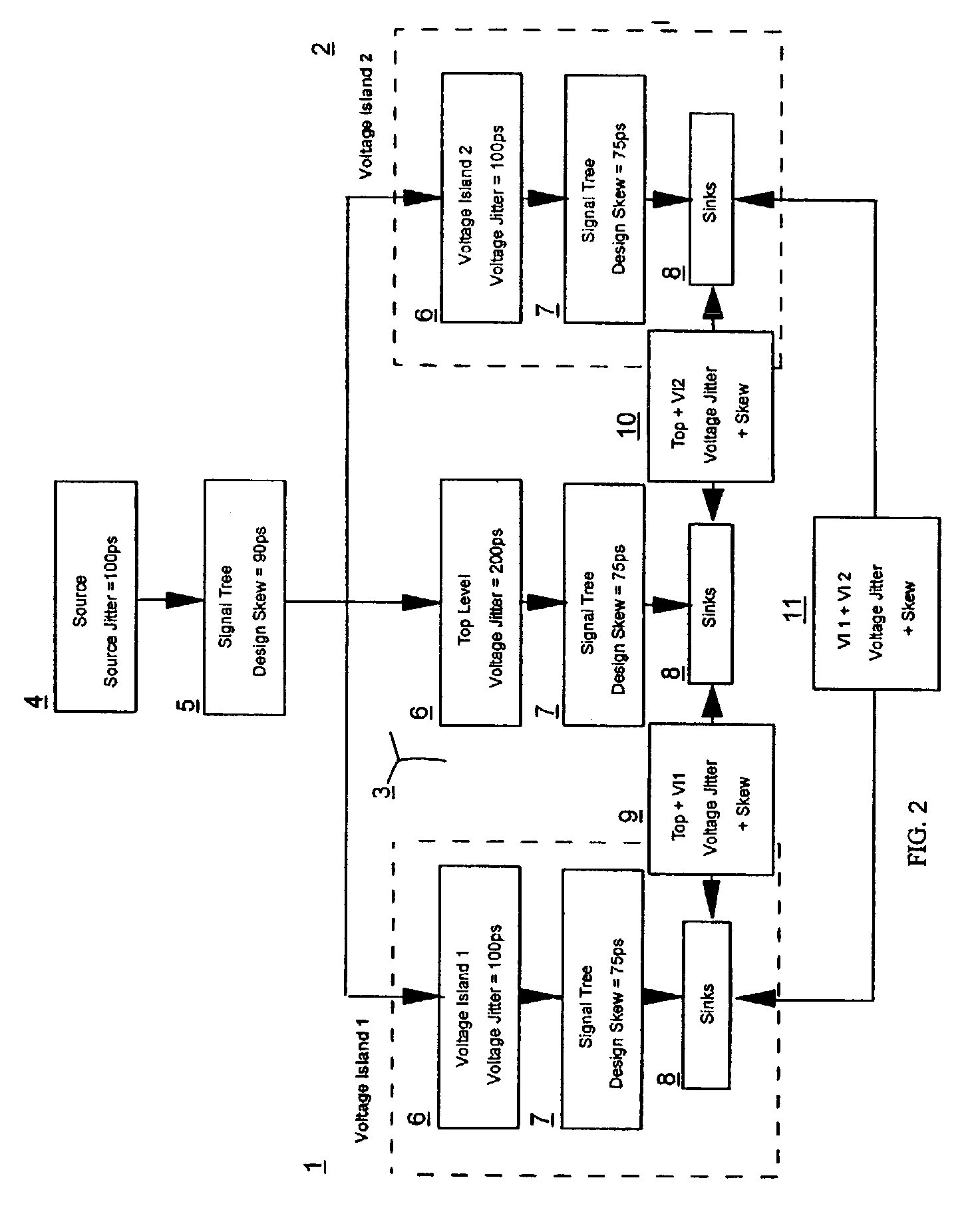
[0014]Voltage Islands complicate signal balancing for two primary reasons: 1) The signal is divided among multiple Random Logic Macros (RLMs) while design, layout and balance routing is performed independently within each RLM. During operation the voltage level within each Voltage Island independently floats between Best Case (BC) and Worst Case (WC) conditions resulting in signal latencies within each Voltage Domain which vary independently of each other over a known range. Signal arrival times can vary by over 20% of the total signal's latency as voltage levels float between BC and WC conditions. The independent floating of voltage levels between separate voltage domains introduces additional skew. As a result, the goal of signal balancing in Voltage Island designs is to balance the signal over all possible combinations of operating conditions, instead of one specific condition.

[0015]FIG. 1 illustrates an example of a signal extending through two voltage domains 1 and 2 and the to...


PUM


Abstract

A method for balancing signals across an IC design having multiple voltage domains. The method uses a voltage tress to balance the signals at the top level above the voltage domains. Then using worst case and best case signal latencies determines the average latency in each voltage domain. Then balancing signals at the other levels of the design by incrementing the latencies in each domain until a target level based on the slowest average latency is reached.

Description

CROSS REFERENCE TO RELATED APPLICATIONS[0001]This application is related to another U.S. patent application Ser. No. 10 / 248,301 IBM Docket Number BUR920020136US1, entitled “Programmable Delay Method for Hierarchical Signal Balancing,” which is filed concurrently with this application by the same assignee and is incorporatated herein by reference.BACKGROUND OF THE INVENTION[0002]1. Field of the Invention[0003]This invention relates generally signal balancing, specifically to a method, system and software for balancing signals spanning multiple voltage domains.[0004]2. Background of the Invention[0005]The semiconductor industry is constantly increasing the number of circuits and functionality that can be compressed onto a single die. As process dimensions decrease, this ability has grown at an astronomical rate. The ability to put entire functioning systems on a single die is now the norm rather than the exception. As a consequence of this growth, the die / integrated circuit can be vie...

Claims


Application Information

Patent Timeline
Patent Type & Authority Patents(United States)
IPC IPC(8): G06F9/45G06F17/50G06K19/077H01L21/82H01L21/822H01L27/04
CPCG06F17/5045G06F30/30G06K19/077
Inventor FRY, THOMAS WALKERMENARD, DANIEL RICHARDNORMAND, PHILLIP PAUL
Owner MARVELL ASIA PTE LTD
Why Eureka
Eureka Blog
Learn More