Termination impedance tuning circuit
a technology of impedance tuning and termination impedance, which is applied in logic circuits, pulse techniques, and reliability increasing modifications, etc., can solve the problems of limited range over which the scheme may be tuned, and the accuracy of the scheme can be limited, so as to achieve precise termination impedance and reduce fabrication costs
- Summary
- Abstract
- Description
- Claims
- Application Information
AI Technical Summary
Benefits of technology
Problems solved by technology
Method used
Image
Examples
embodiment 100
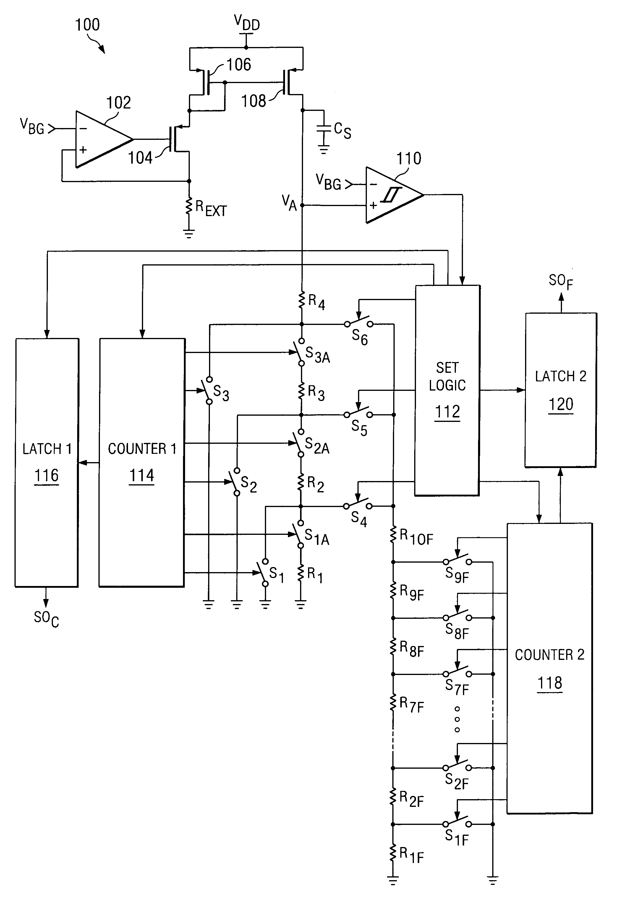
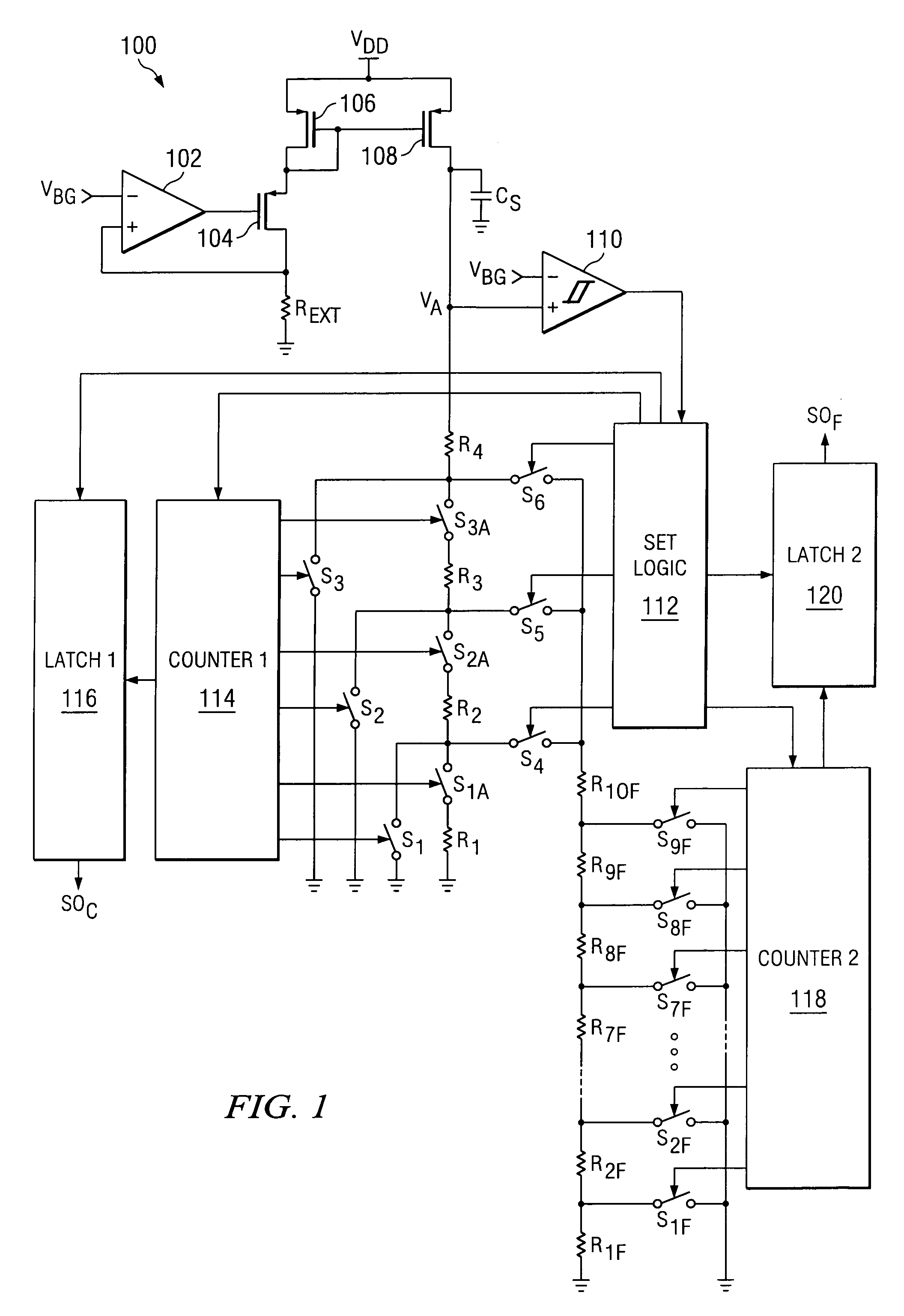
[0010]FIG. 1 is a circuit diagram of a calibration system of a first preferred embodiment 100 of the present invention. An opamp 102 is provided, having a bandgap voltage VBG provided to its non-inverting input. Its output is connected to the gate of an NMOS transistor 104. The drain of transistor 104 is connected to one port of a precision external resistor REXT, the other port of which is connected to ground, and to the inverting input of opamp 102. The drain of transistor 104 is connected to an input side of a current mirror comprised of NMOS transistors 106 and 108. The current mirror is connected to the power supply at VDD. This provides a reference current for programmable resistor bridges, discussed below, that is stabilized with respect to temperature, process and supply voltage.
[0011]The output side of the current mirror is connected to a switched series bridge of resistors R1, R2, R3 and R4, for coarse tuning, with one port of resistor R1 being connected to ground, and hav...
embodiment 200
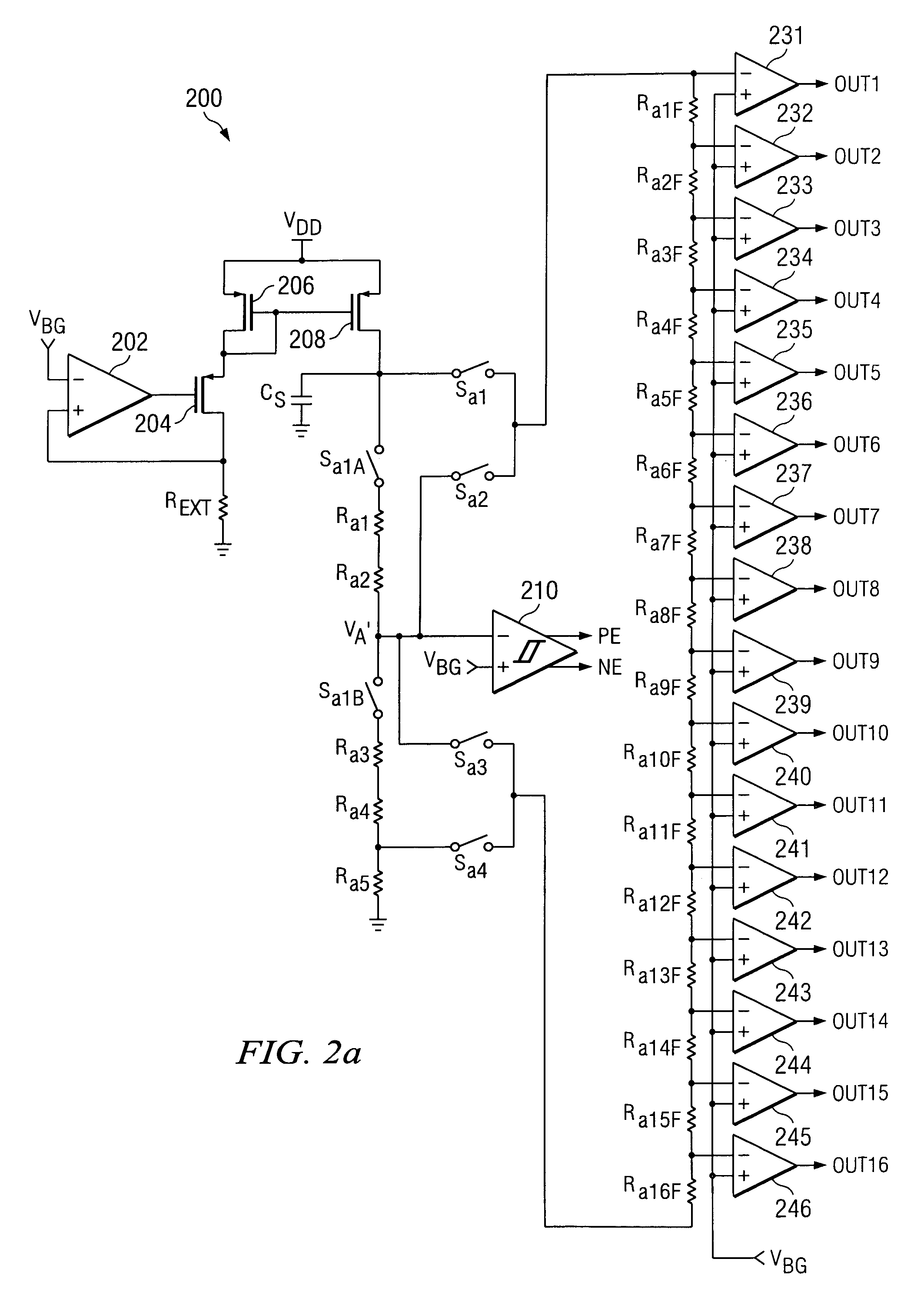
[0018]A second preferred embodiment 200 of a calibration system according to the present invention is shown in FIGS. 2a and 2b. System 200 represents an improvement over system 100, as it continuously calibrates the termination impedance. In system 200, circuit elements 202, 204, REXT, 206, 208 and CS are the same as circuit elements 102, 104, REXT, 106, 108 and CS of system 100, and operate in the same way as described above for them.
[0019]In system 200, the output side of the current mirror is connected to one port of a switch Sa1A, the other port of which is connected to one end of a series pair of resistors Ra1 and Ra2. The output side of the current mirror is also connected to a first port of a switch Sa1. The other end of the series pair of resistors Ra1 and Ra2 is connected to node VA′, which is the inverting input of a comparator 210, with comparator 210 having one-sided hysteresis of 50 mV. A bandgap voltage VBG is connected to the non-inverting input of opamp 210. Comparat...
PUM
 Abstract
Description
Claims
Application Information
 - R&D
- Intellectual Property
- Life Sciences
- Materials
- Tech Scout
- Unparalleled Data Quality
- Higher Quality Content
- 60% Fewer Hallucinations
Browse by: Latest US Patents, China's latest patents, Technical Efficacy Thesaurus, Application Domain, Technology Topic, Popular Technical Reports.
© 2025 PatSnap. All rights reserved.Legal|Privacy policy|Modern Slavery Act Transparency Statement|Sitemap|About US| Contact US: help@patsnap.com


