
High-reliability shift register circuit

a shift register and high-reliability technology, applied in the direction of static storage, digital storage, instruments, etc., can solve the problems of complex manufacturing process and electrical characteristics, complex manufacturing process, and needing three clock-pulse signals in the whole shift register circui

Active Publication Date: 2005-11-29
WINTEK CORP
View PDF4 Cites 104 Cited by
  • Summary
  • Abstract
  • Description
  • Claims
  • Application Information

AI Technical Summary

Benefits of technology

[0012]Therefore, the main purpose of the current invention is to avoid the malfunctioning situation for the shift register circuit resulting from the a-Si TFT under applied stress.
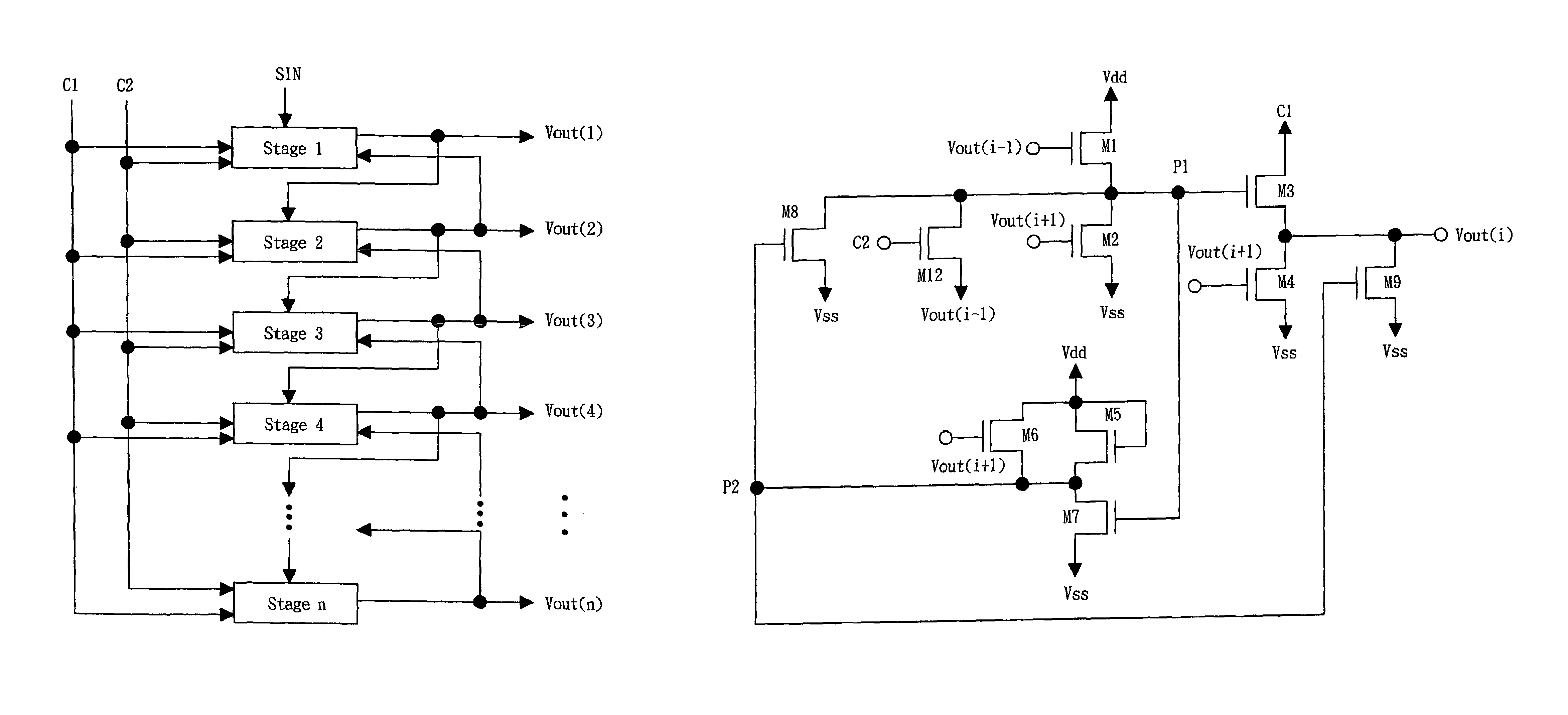
[0014]The shift register of this invention is composed of several stages (Stage 1˜Stage n). The stages are connected in serial and send the output signals Vout(1)˜Vout(n) to the load, for example, the panel. Initially, a serial-in signal SIN is fed into the Stage 1, and input signals for the rest stages are from the output signal of the next-former stage individually. The shift register is controlled by two clock-pulse signals, C1 and C2, which are out of phase. Each stage consists of nine transistors. The main circuit of each stage of the shift register circuit is composed of transistors M1˜M4, and the turn-on time for the four transistors are only 1˜2 pulse time within one frame time. Transistors M5 and M7 construct an inverter circuit which continuously offers a high-level supply voltage Vdd that controls activities of transistors M8 and M9 so as to continuously offer a low-level supply voltage Vss to the first node P1 and the output terminal Vout(i) such that the first node P1 and the output terminal Vout(i) being in a floating state is avoided.
[0015]By way of this, even threshold voltages (Vth) for transistors M8 and M9 keep increasing because of the sustained stress, the steady-state saturation current supplements moderately so as to avoid mis-actions of node P1 and output terminal Vout(i) affected by clock-pulse signal or other noises.

Problems solved by technology

The major difference between a LTPS TFT and an a-Si TFT is the complexity of manufacturing process and the electrical characteristics.
A LTPS TFT has a higher carrier-mobility whereas its manufacturing process is more complicated.
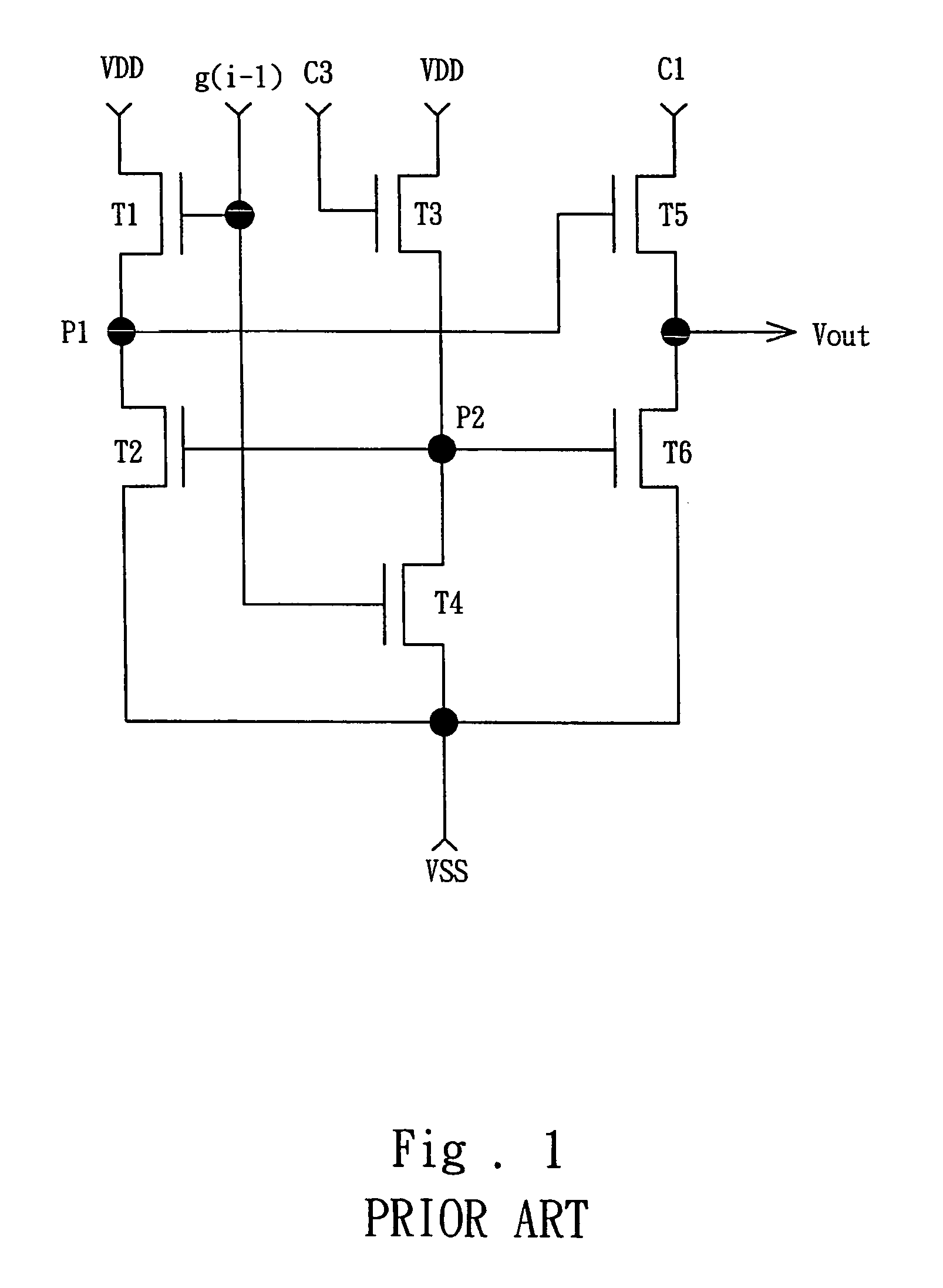
The defect of Prior Art U.S. Pat. No. 5,222,082 is that the whole shift register circuit needs three clock-pulse signals to complete the function.
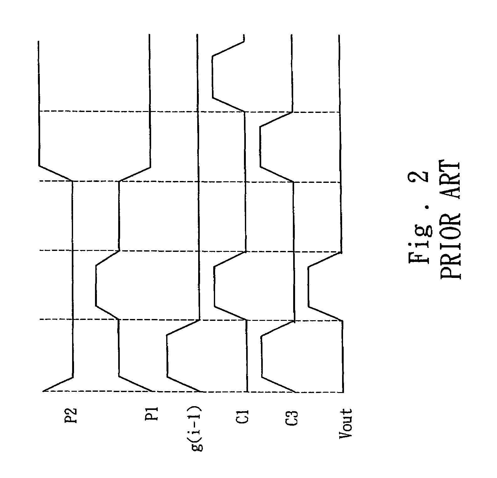
Moreover, nodes P1 and P2 of the circuit will be in a floating state for a short time, which results in circuit mis-actions due to nodes P1 and P2 are affected by clock-pulse signal or other noises.
Besides, threshold voltages (Vth) for TFT T2, T3, and T6 increase because of the sustained stress, which leads to the circuit fails at last.
However, in the shift register circuit of the U.S. Pat. No. 3,937,984, node P1 will be in a floating state for a short time, which results in the circuit mis-action of TFT turn-on due to nodes P1 is affected by clock-pulse signal or other noises.
Besides, threshold voltages (Vth) for TFT T1 and T3 increase because of the sustained stress, which leads to the circuit fails at last.

Method used


Image

  • High-reliability shift register circuit
  • High-reliability shift register circuit
  • High-reliability shift register circuit

Examples


Embodiment Construction

[0034]Please refer to FIGS. 5 and 6, which are the block diagram of the shift register and the schematic circuit for the 1st embodiment of the current invention. As shown in figures, the shift register is composed of several stages (Stage 1˜Stage n). The stages are connected in serial and send the output signals Vout(1)˜Vout(n) to gate lines of the panel. Initially, a serial-in signal SIN is fed into the first stage (Stage 1), and input signals for the rest stages are from the output signal of the next-former stage Vout(1)˜Vout(i−1) respectively. The shift register circuit is controlled by two clock-pulse signals, C1 and C2, which are out of phase, where C1 controls odd stages and even stages are controlled by C2.

[0035]The inner circuit of odd stages includes the first one transistor M1 whose gate connects to the output signal of the next-former stage Vout(i−1) and the drain connects to the high-level supply voltage Vdd; the second one transistor M2 whose gate connects to the output...


PUM


Abstract

The main circuit of each stage of the high-reliability shift register circuit is composed of transistors, and the turn-on time for the four transistors are only 1˜2 pulse time within one frame time. Transistors construct an inverter circuit which continuously offers a high-level supply voltage that controls activities of transistors so as to continuously offer a low-level supply voltage to the first node and the output terminal such that avoids the first node and the output terminal being in a floating state. Besides, one of the transistor acts as a charging circuit that extends the lifetime of another transistor. This circuit avoids the affection on the behavior of the shift register circuit that is caused by an a-Si (amorphous silicon) TFT under a sustained stress.

Description

FIELD OF THE INVENTION[0001]The present invention relates to a high-reliability shift register circuit and more particularly to a manufacturing process technology for the a-Si TFT, which avoids the malfunctioning situation for the shift register circuit resulting from the a-Si TFT under applied stress.BACKGROUND OF THE INVENTION[0002]The SOG (system on glass) technology can be actualized by technologies of a-Si and LTPS (low temperature poly-silicon). The major difference between a LTPS TFT and an a-Si TFT is the complexity of manufacturing process and the electrical characteristics. A LTPS TFT has a higher carrier-mobility whereas its manufacturing process is more complicated. By contrast, a-Si TFT has a lower carrier-mobility than LTPS, but its manufacturing process is simpler and well developed, and therefore an a-Si TFT has a better competitiveness in terms of cost.[0003]Accordingly, due to the limit of manufacturing ability, the threshold voltage (Vth) for the manufactured a-Si...

Claims


Application Information

Patent Timeline
IPC IPC(8): G11C19/00G11C19/28
CPCG11C19/282
Inventor WANG, WEN-CHUNLIAO, WEN-TUITSAI, JA-FU
Owner WINTEK CORP
Learn More