
Device for measuring surface defects

a technology for measuring devices and defects, applied in liquid/fluent solid measurement, instruments, machines/engines, etc., can solve problems such as impairing measuring accuracy, affecting the accuracy of measuring, and particularly sensitive apparatuses to small particles

Inactive Publication Date: 2005-10-11
ONTO INNOVATION INC
View PDF29 Cites 14 Cited by
  • Summary
  • Abstract
  • Description
  • Claims
  • Application Information

AI Technical Summary

Benefits of technology

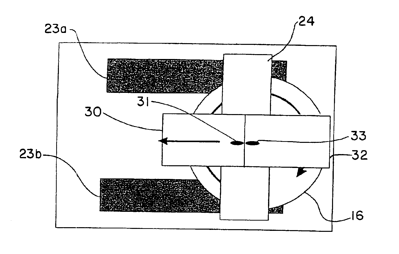
[0015]The device according to the invention for measuring surface defects, comprising a sample holder, a rotation drive for the sample holder with its rotational axis perpendicular to the sample surface to be measured, an optical measuring system for scattered light measurements, as well as at least one linear drive for the measuring system with its rotational direction radial to the rotational axis of the sample holder, is capable of scanning the entire sample surface. By not only moving the sample, but also the measuring system, less space is needed as a whole and the entire device can be constructed in a more compact form. This makes the device particularly suitable for process-oriented quality surveillance, since it can simply be integrated into existing process facilities.
[0030]It may also be advantageous to dispose a light wave guide downstream from the light source. This allows the light source as such to be spatially removed from the other components of the optical measuring system. In this way, the optical measuring system can be miniaturized and / or be designed in compact construction without becoming subject to excessive limitation in the selection of the light source. The use as light wave guide also makes it easer to set up any kind of incidence geometry in the proximity of the sample. Downstream from the light wave, as well, a light deflecting unit may be provided.

Problems solved by technology

Due to the very large acceptance angle, this apparatus is particularly sensitive to small particles.
This apparatus however has the disadvantage that scattered light is generated also at both converging lenses, which as a whole corrupts the measuring results.
With this method, the sample is either rotated around its axis while simultaneously undergoing a translational movement in radial direction and while the light beam remains stationary, or the sample remains immobile and the spiral-form movement is executed by the light beam, which in very sensitive optical systems impairs the measuring accuracy.
The apparatus already on the market has the disadvantage that the measuring head has to be kept very small, in order to allow for the swinging motion.
Since blue lasers require more space, the resolution cannot be further improved in these devices.

Method used


Image

  • Device for measuring surface defects
  • Device for measuring surface defects
  • Device for measuring surface defects

Examples


Embodiment Construction

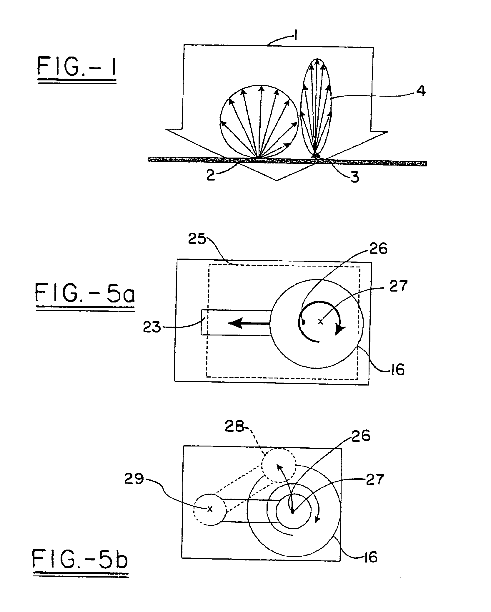
[0047]FIG. 1 shows the differing scatter characteristics of particles of differing sizes. Incident light 1 falls on a small particle 2 as well as on a large particle 3. A particle is considered small when its size is much smaller than the wavelength of the incident light 1. A particle is considered large when its size is comparable to the wavelength of the incident light 1 or even greater. The scatter characteristics of small particles 2 and large particles 3 differ in so far as the small particle 2 scatters in isotropic manner into the space, while the large particle 3 generates strong backscattering.

[0048]FIG. 2 shows an optical measuring system for the detection of large particles in the form of a measurement block 10 for measuring samples such as wafers 16. The wafer 16 is supported by a sample holder (wafer chuck) 17 which is caused by a rotation motor 18 to rotate around the axis 27 perpendicularly to the wafer surface 16. The arrows indicate the possible directions of movemen...


PUM

PropertyMeasurementUnit
depthaaaaaaaaaa
surface defectsaaaaaaaaaa
optical measuringaaaaaaaaaa

Abstract

In view of the miniaturization of semiconductor components, the prevention of particles and other defects on the wafer surface during production is of great importance. The inspection should proceed as process-oriented as possible. For this purpose, devices are needed which on the one hand, are of very compact construction, while on the other hand, they still are equipped with measuring systems meeting the highest requirements.The device according to the invention for measuring surface defects, comprising a sample holder, a rotation drive for the sample holder, wherein the rotational axis runs perpendicular to the sample surface to be measured, an optical measuring system (10) for measuring scattered light, as well as at least one linear drive (23) for the measuring system, wherein the rotational direction is radial to the rotational axis of the sample holder, is capable of scanning the entire sample surface (16). By moving not only the sample, but also the measuring system, the need for space as a whole is reduced and the total device can be constructed with a more compact design.

Description

CROSS REFERENCE[0001]This application is a Continuation-In-Part of U.S. Ser. No. 10 / 120,641, filed Apr. 11, 2002, now U.S. Pat. No. 6,798,513, for Measuring Module, herein fully incorporated by reference.FIELD OF THE INVENTION[0002]The invention relates to a device for measuring surface defects.[0003]In view of the miniaturization of semiconductor components, the prevention of particles and other defects on the wafer surface during production is of great importance. Since a particle grain can by now be larger than an entire circuitry, even the smallest defects lead to a large amount of waste.BACKGROUND OF THE INVENTION[0004]In general, scattered light is used for measuring defects on smooth surfaces. For this purpose, the surface of, for example, a wafer is illuminated with a laser beam. The scatter characteristics of different particle sizes are shown in FIG. 1. A small particle 2 as well as a large particle 3 are illuminated with a laser beam 1. ‘Small particle’ means that the par...

Claims


Application Information

Patent Timeline
Patent Type & Authority Patents(United States)
IPC IPC(8): G01F23/284G01N21/47G01N21/21G01N21/88G01N21/95G01Q30/02G01Q60/00
CPCG01F23/284G01N21/211G01N21/47G01N21/9501
Inventor ABRAHAM, MICHAELLANG, ANDREASSCHWEIGER, MICHAEL
Owner ONTO INNOVATION INC
Learn More