Method to fabricate multi-level silicon-based microstructures via use of an etching delay layer

a technology of silicon-based microstructures and delay layers, which is applied in the direction of microstructures, microstructure devices, coatings, etc., can solve the problems of affecting the desired motion of the components of the device, and affecting the stability of the devi

Active Publication Date: 2005-08-16
NAT TECH & ENG SOLUTIONS OF SANDIA LLC
View PDF2 Cites 12 Cited by
  • Summary
  • Abstract
  • Description
  • Claims
  • Application Information

AI Technical Summary

Benefits of technology

[0010]New methods for fabrication of silicon-based microstructures have been developed. These methods comprise the deposition and pa

Problems solved by technology

Gross assembly steps require precision handling, positioning, and bonding of delicate millimeter-scale structures, which are fraught with opportunities for failure.
In particular, when the goal is a micromechanical device, the bonding materials can easily interfere with the desired motion of the components of the device.
Similarly, when the goal is a microfluidic device, the bonding materials can block the flow channels, or prevent microvalves from functioning properly.
Working against the above motivations for direct fabrication of complex microstructures is the difficulty of fabricating such microstructures in their entirety.
As the complexity of a process required for fabrication of a desired silicon microstructure increases, the useful yield of that process falls rapidly toward zero.
Complex fabrication processes are not only susceptible to error, but in many cases can lead to accumulation of residual stress, nonplanarity, and other structural flaws which can render the desired product unusable.

Method used


Image

  • Method to fabricate multi-level silicon-based microstructures via use of an etching delay layer
  • Method to fabricate multi-level silicon-based microstructures via use of an etching delay layer

Examples


Embodiment Construction

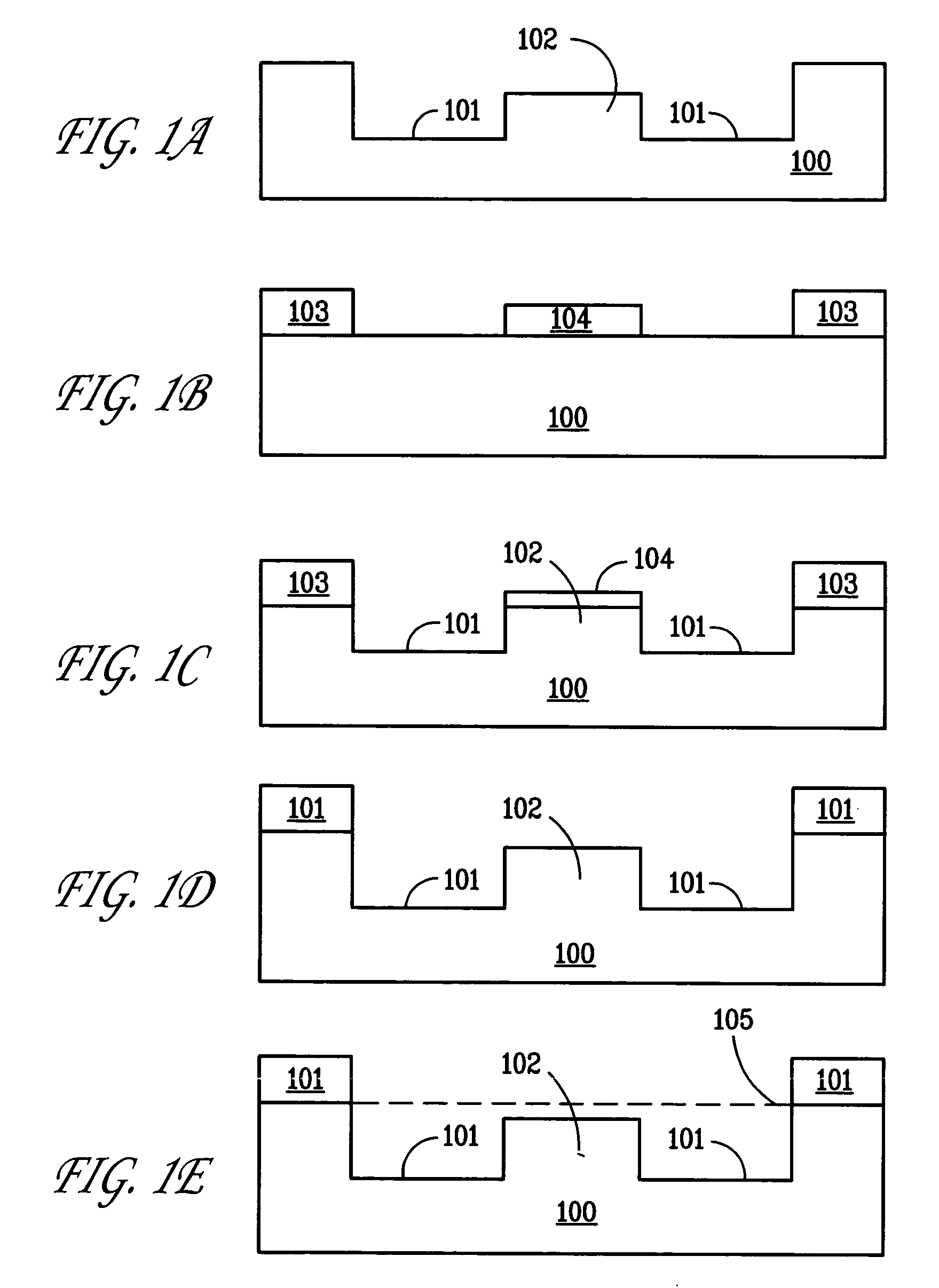
[0012]To etch structural features to different depths in a single etching step, an etching delay layer of a predetermined thickness can be placed over the features for which smaller etching depth is desired. FIG. 1 shows structures resulting in various stages of fabricating structural features with different depths using the present invention.

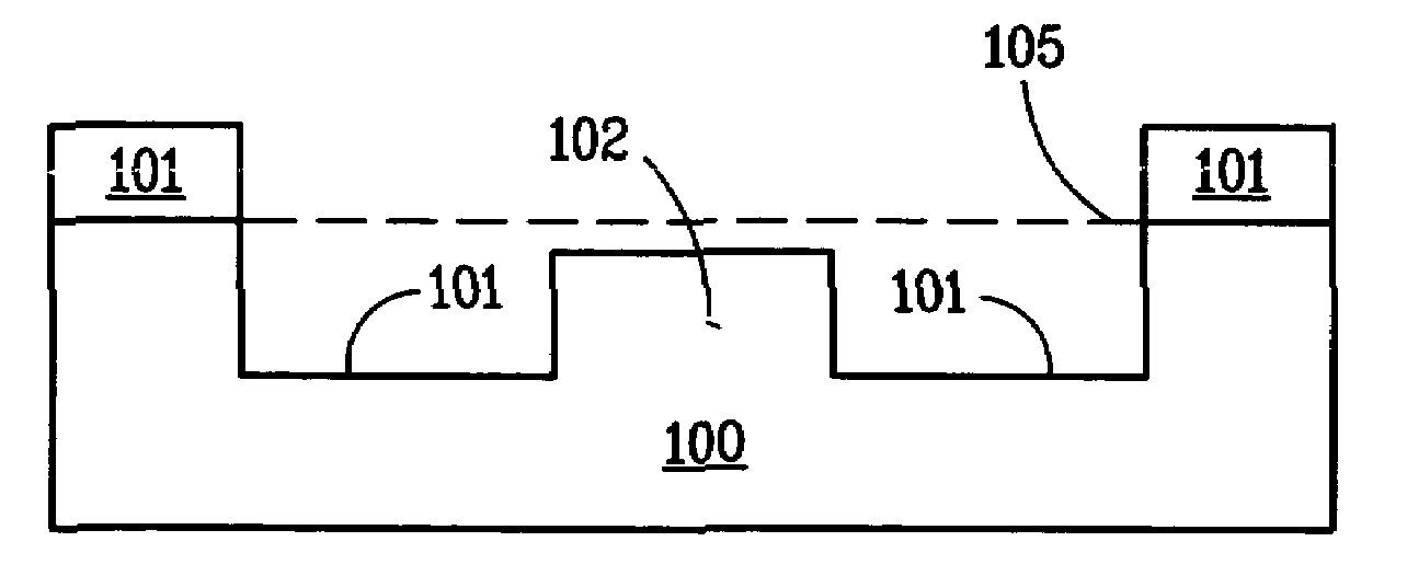
[0013]FIG. 1a shows a desired microcomponent comprising a substrate 100, within which has been defined a well 101 with a central protrusion 102. Assume for clarity that the structure in the illustration is rotationally symmetric about a central vertical axis.

[0014]FIG. 1b shows substrate 100 before the etching process is begun. Mask layer 103 substantially prevents etching from occurring in the region outside of the well 101 to be fabricated. Central protrusion 102 results from limiting the etching action in substrate 100 at the desired location of said central protrusion. This is accomplished by depositing an etching delay layer 104 atop subst...


PUM

PropertyMeasurementUnit
Thicknessaaaaaaaaaa
Microstructureaaaaaaaaaa
Depthaaaaaaaaaa

Abstract

New methods for fabrication of silicon microstructures have been developed. In these methods, an etching delay layer is deposited and patterned so as to provide differential control on the depth of features being etched into a substrate material. Structures having features with different depth can be formed thereby in a single etching step.

Description

GOVERNMENT RIGHTS[0001]This invention was made with Government support under Contract DE-AC04-94AL85000 awarded by the U.S. Department of Energy. The Government has certain rights in the invention.FIELD OF THE INVENTION[0002]The present invention relates generally to silicon-based microstructure fabrication, and in particular to the use of etching delay layers in fabrication of multi-level silicon-based microstructures.BACKGROUND OF THE INVENTION[0003]Development of new fabrication technologies for silicon-based microstructures is currently under aggressive pursuit. Silicon-based microstructures commonly comprise silicon and silicon oxides, but can also comprise silicon nitride, metal thin films, and a range of other structural materials known in the art. Such microstructures are commonly fabricated using a range of techniques originally developed for fabrication of silicon integrated circuits, and find application in the area of microelectromechanical systems (MEMS), and in microfl...

Claims


Application Information

Patent Timeline
IPC IPC(8): H01L21/02H01L21/302B81C1/00H01L21/308
CPCH01L21/3083B81C1/00626B81C2201/0142
Inventor MANGINELL, RONALD P.SCHUBERT, W. KENTSHUL, RANDY J.
Owner NAT TECH & ENG SOLUTIONS OF SANDIA LLC
Why Eureka
Try Eureka