Liquid crystal display device

Active Publication Date: 2005-08-09
PANASONIC LIQUID CRYSTAL DISPLAY CO LTD +1
View PDF2 Cites 16 Cited by
  • Summary
  • Abstract
  • Description
  • Claims
  • Application Information

AI Technical Summary

Benefits of technology

[0006]IPS-type liquid crystal display devices are low in aperture ratio, and, thus there is a used for improvements which will offer a higher aperture ratio, that is, a higher optical transmissivity. Typically, pixels are designed to have a comb-like electrode structure using a single pixel electrode in an area that is interposed between common electrodes—in other words, a structure in which each pixel is bisected. However, the inventors' study has revealed that structures with a pixel divided into more than four parts require special designs for reducing display defects, such as cross-talk, while at the same time further increasing the aperture ratio.
[0007]The present invention, as disclosed herein, provides an approach to solve the newly found problems stated above, and an object of this invention is to further increase the aperture ratio, while simultaneously reducing the problem of operation failure and crosstalk that are unique to an IPS display-mode liquid crystal display device. Such a device has a common electrode overlying a drain wiring line, with an organic film laid therebetween, and also has a pixel electrode over the organic film, while having more than four open regions that arc surrounded by the common and pixel electrodes in a cross-sectional structure transverse to part between neighboring drain wiring lines.

Problems solved by technology

However, compared to display devices of the type using twisted nematic (TN) methods, this approach suffers from various problems; for example, it is difficult to enlarge the aperture ratio of picture elements or “pixels”, and, the light utilization efficiency remains low in value.
This backlight luminance increase makes it difficult for an LCD module to achieve low power consumption, such as is required for notebook personal computers (PCs) and handheld or “mobile” electronic tools.

Method used


Image

  • Liquid crystal display device
  • Liquid crystal display device
  • Liquid crystal display device

Examples


embodiment 1

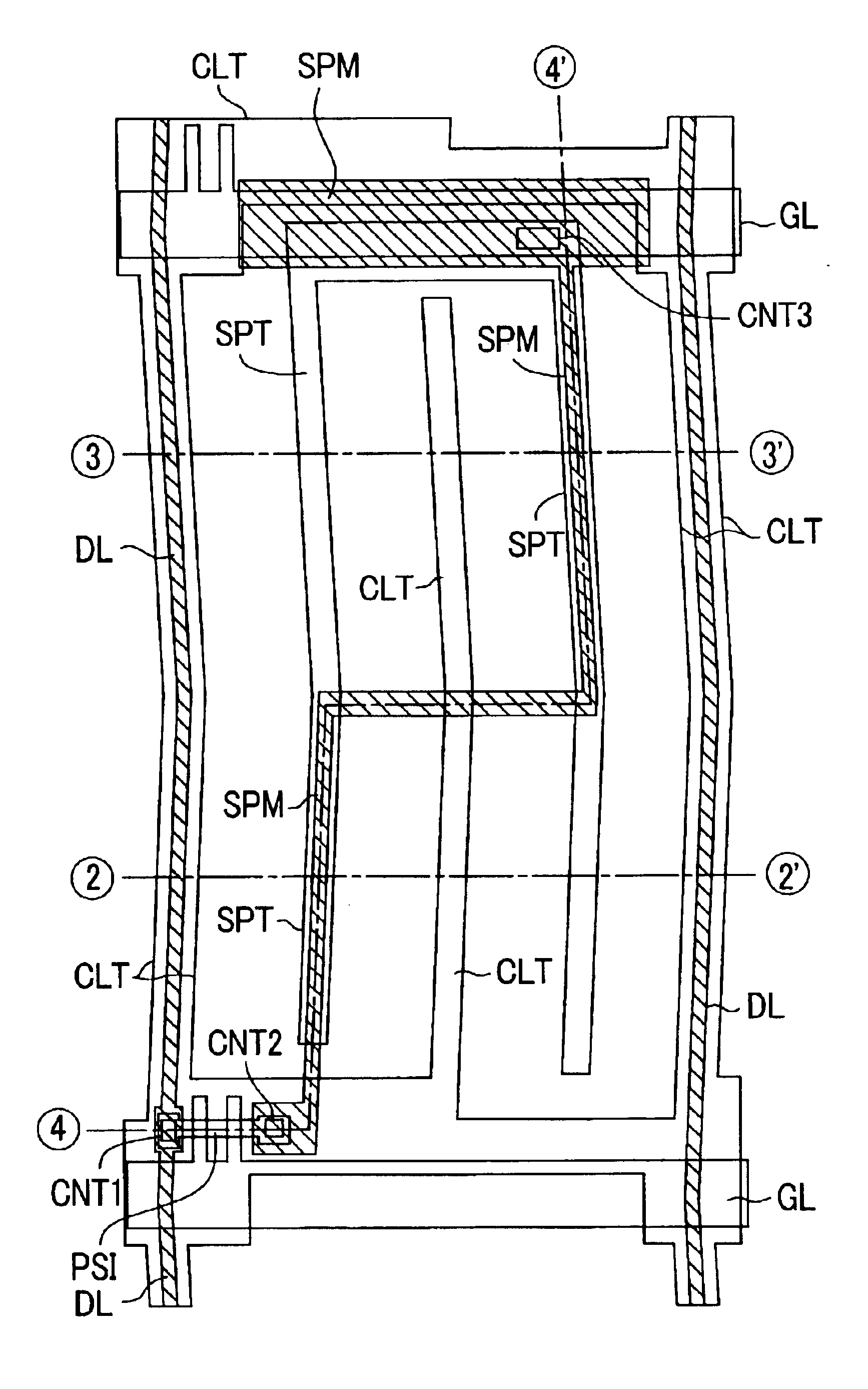
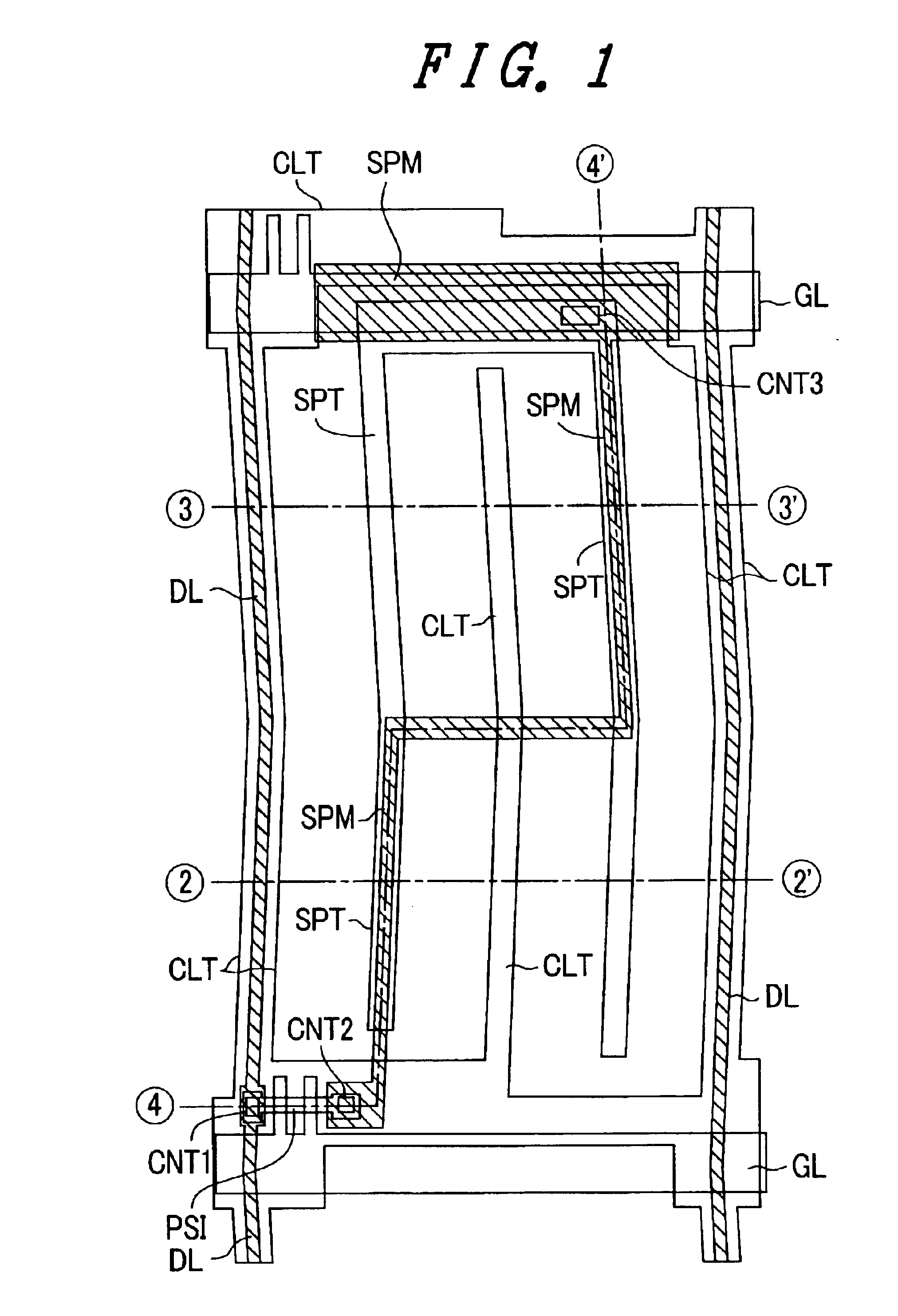
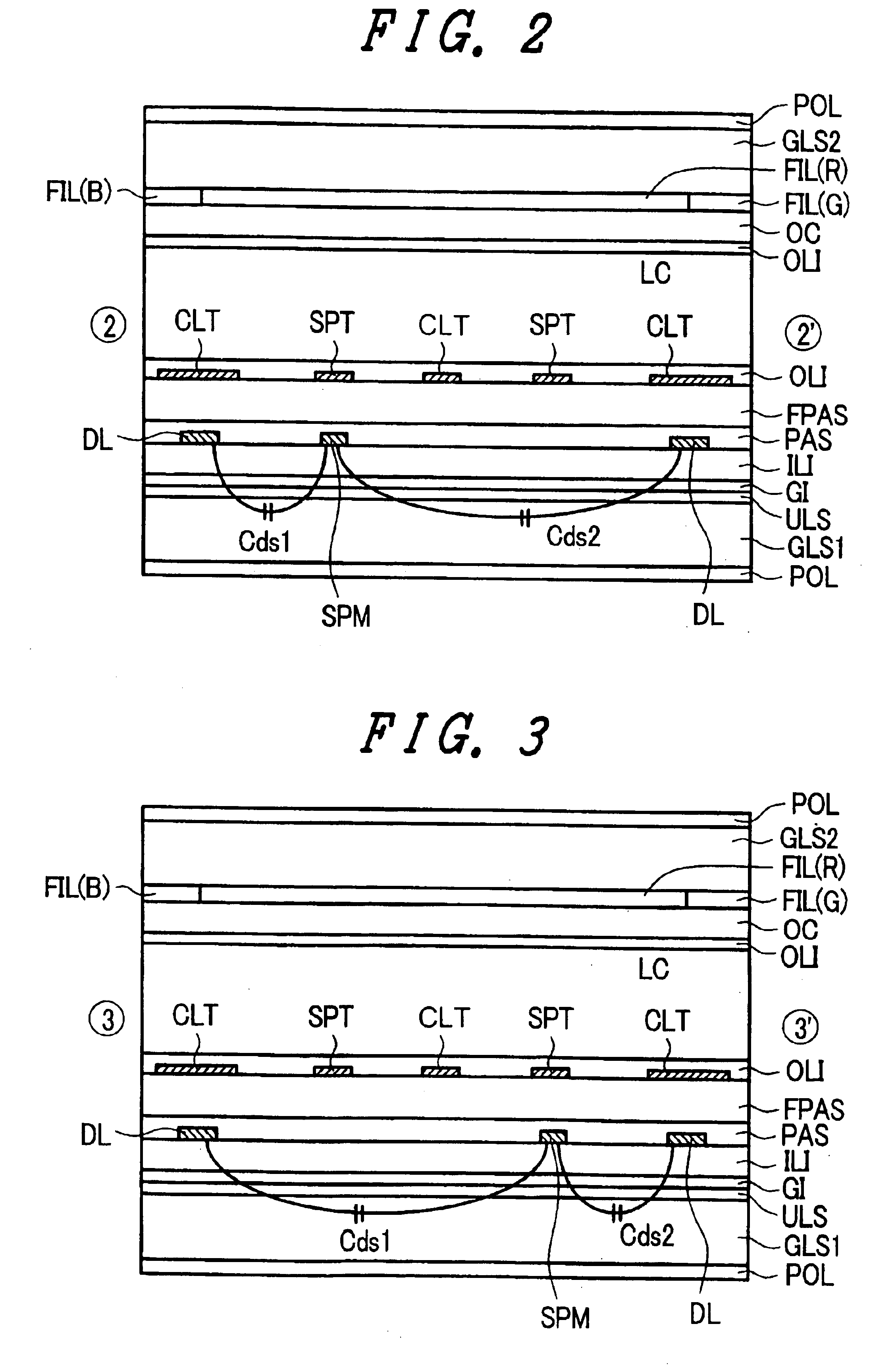
[0022]FIG. 1 is a plan view of one of the pixels (picture elements) of a liquid crystal display device in accordance with one embodiment of the invention, and FIGS. 2 through 4 are cross-sectional views of the pixel as seen along lines 2-2′, 33′ and 4-4′, respectively, in FIG. 1. In these drawings, the numerals indicative of section lines are encircled for purposes of providing visual emphasis of the indicated sections. Note that these drawings indicate a main part of the structure for explanation purposes and that orientation films are eliminated from some of the drawings. Also note that some structure on the opposite or “counter” substrate side also is eliminated in some drawings for purposes of convenience in illustration only.

[0023]FIG. 1 shows a schematic planar pattern of a representative one of the pixels, which pixel is arranged so as to be surrounded by a pair of neighboring gate wiring lines GL and a pair of neighboring drain wiring lines DL. The laser gate wiring line GL ...

embodiment 2

[0059]FIG. 8 is a plan view of a pixel in accordance with a second embodiment of the invention. FIG. 9 shows a cross-section of the pixel as seen along a cut line 99′ in FIG. 8. In these drawings, reference numerals are encircled in order to facilitate an identification of the section line. In addition, reference characters of the upper and lower gate wiring lines GL and right and left drain wiring lines DL which surround a single pixel have suffix numerals appended thereto for purposes of making clearer the order of scanning and the like.

[0060]FIG. 8 shows an IPS scheme pixel pattern having four main transmitting portions arranged in a direction transverse to the drain wiring lines DL in a way similar to the embodiment 1. Its significant feature over the embodiment 1 lies in the configuration and arrangement of the pixel electrode SPM. A single pixel area, which is surrounded by two neighboring gate wiring lines GL1, GL2 and two neighboring drain wiring lines DL1, DL2, is designed ...


PUM


Abstract

In a liquid crystal display device of the active matrix type using in-plane switching (IPS), with at least four transmission regions being formed within a single pixel area surrounded by neighboring gate wiring lines and neighboring drain wiring lines disposed in a direction transverse to the drain wiring lines, a multilayer structure formed of two layers of conductive films with an insulating film sandwiched therebetween is provided at a pixel electrode extending from either one of the neighboring gate wiring lines toward the interior of the pixel and causes one of these two-layer conductive films (i.e. lower pixel electrode placed on the substrate side) is configured to bend or “crank” into a hook-like shape at a central portion of the pixel areas while letting its planar shape be adjacent to one of the neighboring drain lines at the half of the pixel area and also letting it be adjacent to the other of the neighboring drain lines at the other half, thereby widening the viewing angle of an image to be visually displayed on the liquid crystal display device and also brightening the image.

Description

BACKGROUND OF THE INVENTION[0001]The present invention relates in general to liquid crystal display devices and, more particularly, to liquid crystal display devices of the active matrix type in which thin-film transistors (TFT) are used. This invention also relates to a method of manufacture of such devices.[0002]Liquid crystal display devices include the in-plane switching (IPS) type of liquid crystal displays, which are designed to apply a lateral electric field to a liquid crystal gap between upper and lower substrates having a layer of liquid crystal material interposed therebetween. The IPS-mode liquid crystal displays are considered to employ a display scheme that is capable of satisfying the requirements for higher image quality, and they have experienced a variety of improvements in image quality.[0003]In IPS-mode liquid crystal display (LCD) devices, a widely used approach is to employ a scheme for switching liquid crystal orientation by use of a lateral electric field whi...

Claims


Application Information

Patent Timeline
IPC IPC(8): G02F1/13G02F1/1343G02F1/1362G02F1/1368H01L21/3205
CPCG02F1/134363G02F1/136286G02F2001/13629G02F1/13629
Inventor ONO, KIKUOOKE, RYUTAROOCHIAI, TAKAHIRO
Owner PANASONIC LIQUID CRYSTAL DISPLAY CO LTD
Why Eureka
Try Eureka