Spiraling optical device

a spiral optical and optical device technology, applied in the field of spiral optical devices, can solve the problems of increasing the size of the optical device, the optical device unavoidably is horizontal, and the optical device unavoidably has an increased horizontal length, so as to reduce the space for arranging

Inactive Publication Date: 2005-07-26
NEC CORP
View PDF17 Cites 20 Cited by
  • Summary
  • Abstract
  • Description
  • Claims
  • Application Information

AI Technical Summary

Benefits of technology

[0031]In view of the above-mentioned problems in the conventional optical circuits, it is an object of the present invention to provide an optical device which is capable of reducing a space for arranging therein a plurality of optical circuits optically connected to one another in multi-stages on a common substrate.

Problems solved by technology

The optical device illustrated in FIG. 2, including the Mach-Zehnder interferometer type optical circuits arranged horizontally in a line, is accompanied with a problem that the optical device unavoidably is horizontally too long with the result in an increase in a size of the optical device.
However, even in the optical device illustrated in FIG. 3, including a plurality of the Mach-Zehnder interferometer type optical circuits arranged in a zigzag configuration, the optical device would unavoidably have an increased horizontal length if the optical device had an increased number of the Mach-Zehnder interferometer type optical circuits.
This results in reduction in a yield at which optical devices are diced out of a substrate, similarly to the optical device illustrated in FIG.
The reduction in such a yield results in an increase in fabrication costs of an optical device.
In addition, since a substrate has unevenness in a profile of an index of refraction, there is unevenness in characteristics in different areas of the substrate.
Hence, the optical device is accompanied further with a problem that it is more difficult to ensure constant quality in optical devices, if those optical devices were to be diced out of a substrate having a larger size.
Though the problems in a Mach-Zehnder interferometer type optical circuit as an example have been explained above, an optical device comprised of a single or a plurality of circuit(s) formed on a common substrate and optically connected to one another would be accompanied with the same problems as mentioned above.

Method used


Image

  • Spiraling optical device
  • Spiraling optical device
  • Spiraling optical device

Examples


first embodiment

[First Embodiment]

[0097]FIG. 4 is a plan view of an optical device in accordance with the first embodiment of the present invention.

[0098]The optical device in accordance with the first embodiment includes a Mach-Zehnder interferometer type optical circuit 111 comprised of a substrate 112, first to third asymmetric Mach-Zehnder interferometer type optical circuit 1131, 1132 and 1133, and first to fourth directional couplers 1161, 1162, 1163 and 1164.

[0099]The first to third asymmetric Mach-Zehnder interferometer type optical circuit 1131, 1132 and 1133 are optically connected in series and arranged in a spiral.

[0100]The first asymmetric Mach-Zehnder interferometer type optical circuit 1131 located closest to a center of the spiral is designed to have a shorter arm 1141 and a longer arm 1151, and is optically connected to an input waveguide 124 through the first directional coupler 1161 and further to the second asymmetric Mach-Zehnder interferometer type optical circuit 1132 through...

second embodiment

[Second Embodiment]

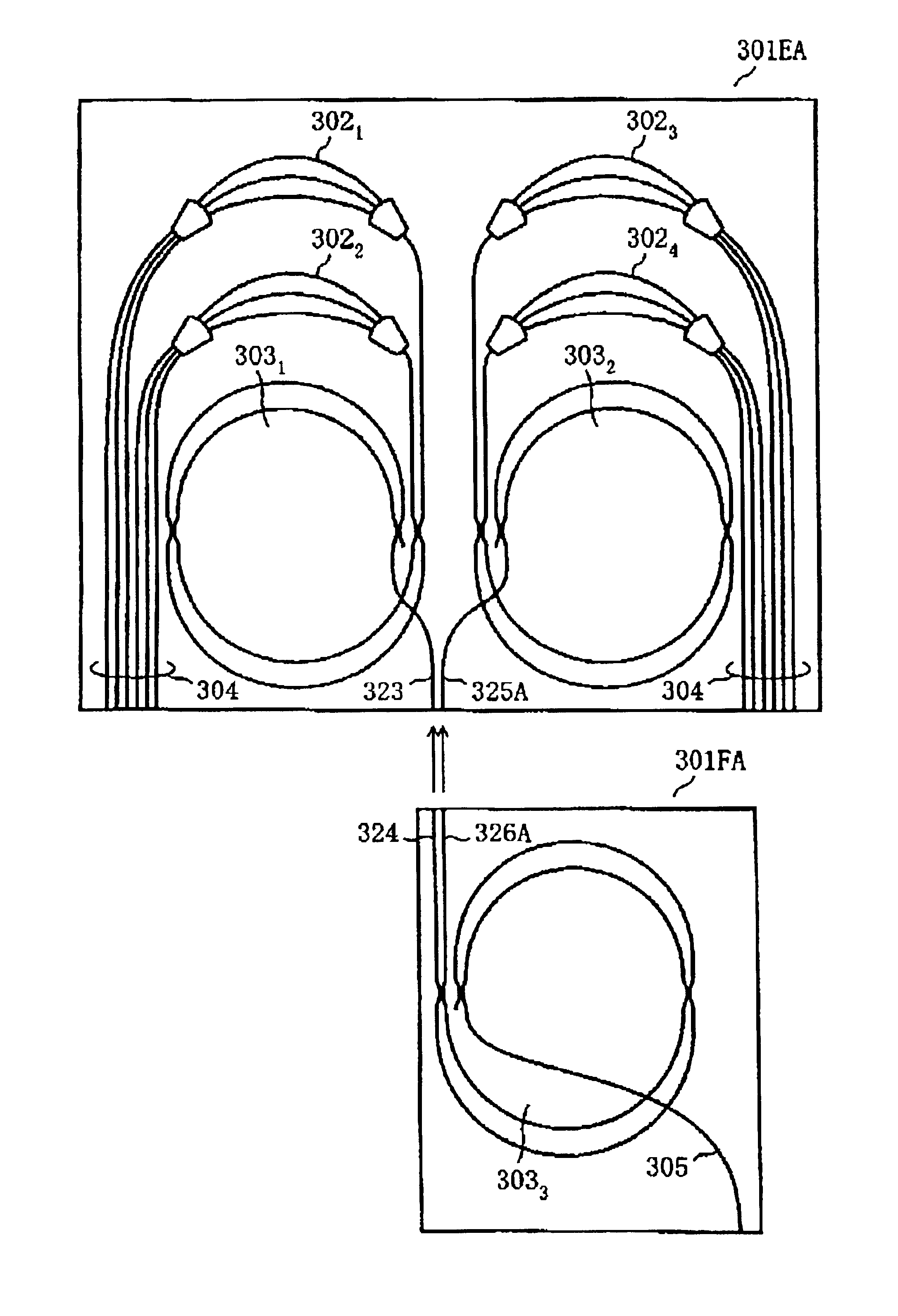
[0136]FIG. 9 is a plan view of an optical device 111A in accordance with the second embodiment of the present invention. Parts or elements that correspond to those of the optical device in accordance with the first embodiment have been provided with the same reference numerals, and operate in the same manner as corresponding parts or elements in the first embodiment, unless explicitly explained hereinbelow.

[0137]The optical device 111A in accordance with the second embodiment is structurally different from the optical device 111 in accordance with the first embodiment in that an input waveguide 124A is optically connected to a shorter arm 1141 of the first asymmetric Mach-Zehnder interferometer type optical circuit 1131.

[0138]The input waveguide 124A optically connects the first directional coupler 1161 to an optical fiber array 151 illustrated with a broken line, and intersects with the shorter arm 1142 and the longer arm 1152 of the second asymmetric Mach-Zehnde...

third embodiment

[Third Embodiment]

[0141]FIG. 10 is a plan view of an optical device in accordance with the third embodiment of the present invention. Parts or elements that correspond to those of the optical device in accordance with the first embodiment have been provided with the same reference numerals, and operate in the same manner as corresponding parts or elements in the first embodiment, unless explicitly explained hereinbelow.

[0142]The optical device in accordance with the second embodiment includes a Mach-Zehnder interferometer type optical circuit 111B1 comprised of a substrate 112, first and second asymmetric Mach-Zehnder interferometer type optical circuit 1131 and 1132, and first to third directional couplers 1161, 1162 and 1163.

[0143]The first and second asymmetric Mach-Zehnder interferometer type optical circuit 1131 and 1132 are optically connected in series and arranged in a spiral.

[0144]The first asymmetric Mach-Zehnder interferometer type optical circuit 1131 located closest to ...


PUM

PropertyMeasurementUnit
angleaaaaaaaaaa
lengthaaaaaaaaaa
lengthaaaaaaaaaa

Abstract

An optical device includes at least one kind of and a plurality of optical circuits optically connected in series wherein the optical circuits are arranged in a spiral on a common substrate.

Description

BACKGROUND OF THE INVENTION[0001]1. Field of the Invention[0002]The invention relates to an optical device, and more particularly to an optical device comprised of an optical unit or a modularized optical unit which optical unit includes a plurality of optical circuits such as a Mach-Zehnder interferometer.[0003]2. Description of the Related Art[0004]It is necessary in a light transmission system to densify an interval between channels or increase a transmission rate in order to increase transmission capacity. A light communication system satisfying such requirement would have to include various optical devices such as a device for merging wavelengths of optical signals into one another or separating a wavelength of an optical signal from merged wavelengths, a device for compensating for dispersion, or a gain equalizer used for an optical fiber amplifier.[0005]Some devices among those optical devices have an optical circuit which is designed to have multi-stages by virtue of planar ...

Claims


Application Information

Patent Timeline
Patent Type & Authority Patents(United States)
IPC IPC(8): G02F1/01G02B6/12G02B6/122G02F1/225G02F1/313
CPCG02B6/12004G02B6/122G02F1/225G02B2006/12159G02F1/0147G02B6/12021
Inventor HATANAKA, TAKAAKI
Owner NEC CORP
Why Eureka
Try Eureka