
Reference current generator, and method of programming, adjusting and/or operating same

a reference current and generator technology, applied in the field of semiconductor memory devices, can solve the problems of parasitic capacitances of interconnection traces or wires as well as the storage cells themselves not being perfectly matched, and the charge state of transistors b>38/b> and b>40/b> decaying over tim

Active Publication Date: 2005-06-28
MICRON TECH INC
View PDF228 Cites 197 Cited by
  • Summary
  • Abstract
  • Description
  • Claims
  • Application Information

AI Technical Summary

Benefits of technology

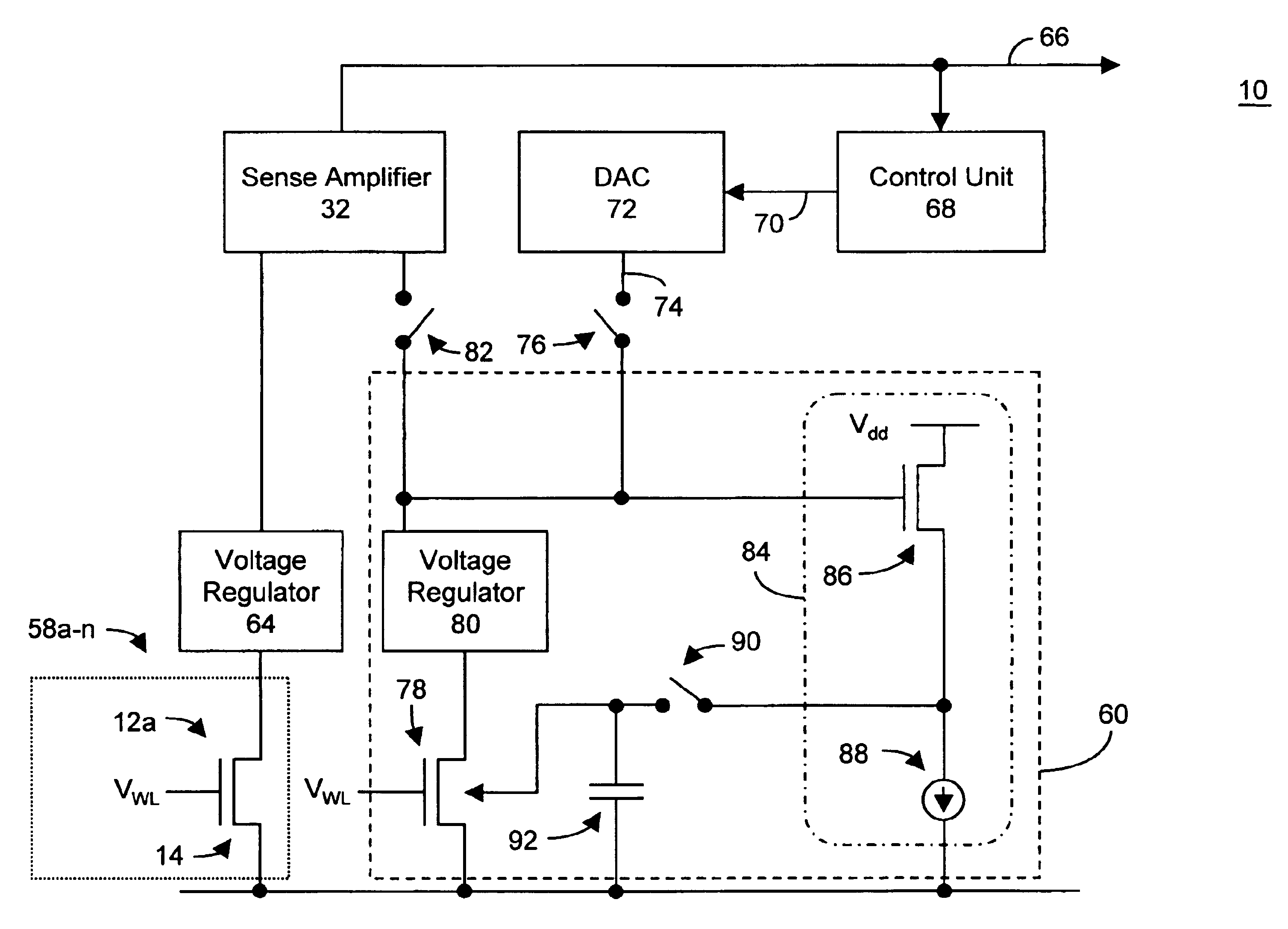
[0015]There are many inventions described and illustrated herein. In a first principal aspect, the present invention is a semiconductor dynamic random access memory device comprising a plurality of bit lines, including a first bit line and a second bit line, and a first digitally controlled reference current generator, selectively coupled to the first bit line, to generate a first reference current in response to a first reference current control word. The memory device also includes a plurality of memory cells, including a first memory cell coupled to the first bit line and a second memory cell coupled to the second bit line. The memory cells store a first data...

Problems solved by technology

However, the reference current generator configuration of FIGS. 3 and 4 suffers from a drawback that the charge state of transistors 38 and 40 decays over time.
In addition, such a conventional configuration also suffers from the disadvantage that the transistors 38 and 40 may often be at a different stage of refresh cycles relative to memory cell 12.
In this way, a data reading uncertainty arises.
Furthermore, the parasitic capacitances of the interconnection traces or wires as well as the storage cells themselves may neither be perfectly matched.
These effects limit the accuracy with which the magnitude of the reference signal can be chosen between the magnitude of the signals representing the logic high data state and the logic low data states.
This is particularly problematic in integrated memory devices of very small transistor size, even if the memory device consists of generally identical transistors.

Method used


Image

  • Reference current generator, and method of programming, adjusting and/or operating same
  • Reference current generator, and method of programming, adjusting and/or operating same
  • Reference current generator, and method of programming, adjusting and/or operating same

Examples


Embodiment Construction

[0055]There are many inventions described and illustrated herein. In a first aspect, the present invention is a technique and circuitry for reading data that is stored in memory cells. In one embodiment of this aspect, the present invention is a technique and circuitry for generating a reference current that is used, in conjunction with a sense amplifier, to read data that is stored in memory cells of a memory device (for example, a DRAM device). The technique and circuitry for generating a reference current may be implemented using an analog configuration, a digital configuration, and / or combinations of analog and digital configurations.

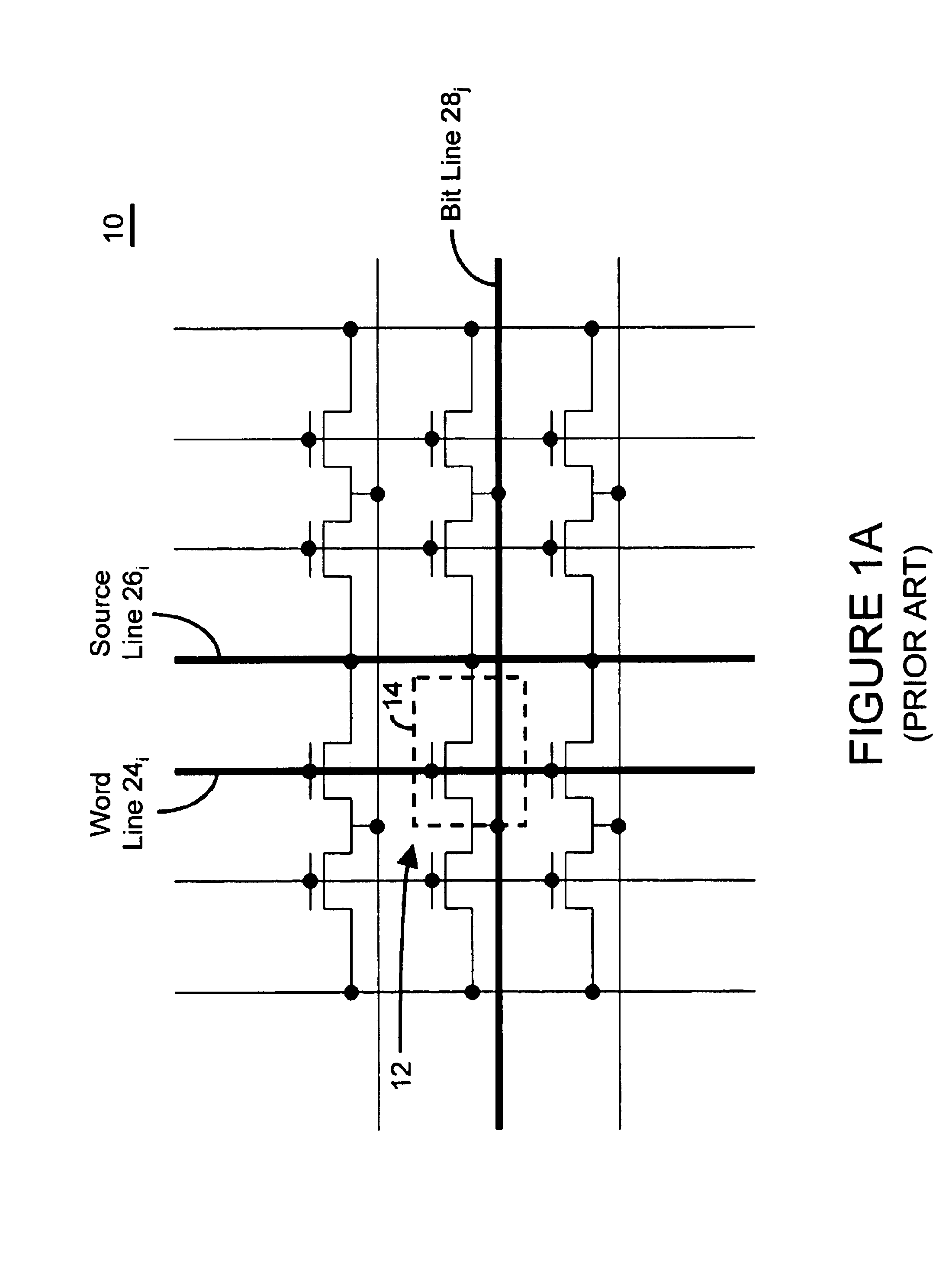
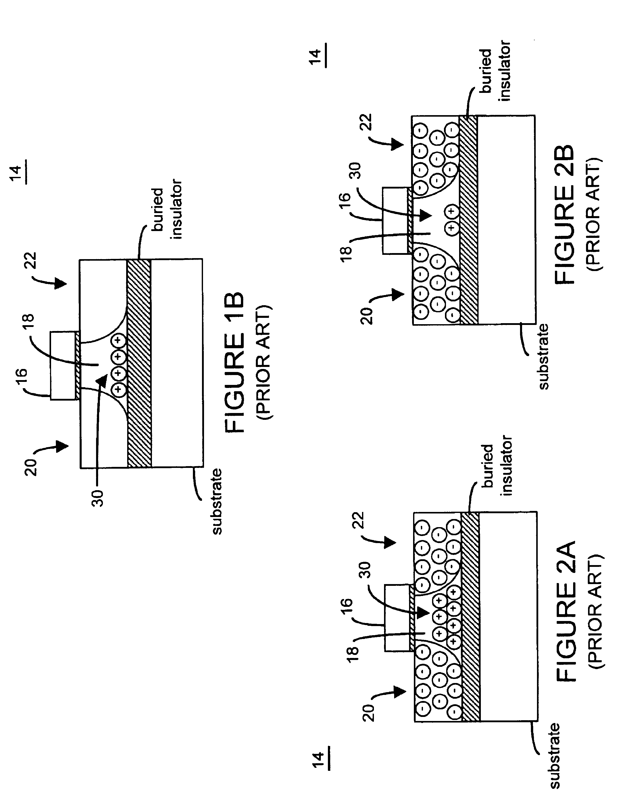
[0056]In one embodiment, the memory cells include one or more transistors, each having an electrically floating body in which an electrical charge is stored. In this regard, the memory cells may be comprised of one transistor which stores an electrical charge in the body region which is representative of a binary state (see, for example, FIGS. 1A, 1...


PUM


Abstract

There are many inventions described and illustrated herein. In a first aspect, the present invention is a technique and circuitry for reading data that is stored in memory cells. In one embodiment of this aspect, the present invention is a technique and circuitry for generating a reference current that is used, in conjunction with a sense amplifier, to read data that is stored in memory cells of a DRAM device. The technique and circuitry for generating a reference current may be implemented using an analog configuration, a digital configuration, and / or combinations of analog and digital configurations.

Description

CROSS-REFERENCE TO RELATED APPLICATIONS[0001]This application claims priority to: (1) U.S. Provisional Application Ser. No. 60 / 470,276, entitled “Method and Apparatus for Generating a Reference Current in a Semiconductor Memory Device”, filed May 14, 2003; and (2) U.S. Provisional Application Ser. No. 60 / 470,462, entitled “An Offset Cancellation Technique—for SOI Capacitor-less 1T DRAM”, filed May 13, 2003 (hereinafter collectively “the Provisional Application”). The contents of the Provisional Applications are incorporated by reference herein in their entirety.BACKGROUND[0002]This invention relates to a semiconductor memory device having a plurality of semiconductor memory cells, and techniques for semiconductor memory cells; and more particularly, in one aspect, to techniques and circuitry for reading data that is stored in memory cells including techniques and circuitry for generating a reference current which is used to read data that is stored in memory cells, of a semiconducto...

Claims


Application Information

Patent Timeline
IPC IPC(8): G11C7/00G11C7/14G11C11/409G11C11/4099G11C29/02G11C16/28
CPCG11C7/14G11C11/4099G11C16/28G11C29/028G11C29/12005G11C29/02G11C11/401G11C2211/4016G11C2029/5006
Inventor PORTMAN, LIONELKAYAL, MAHERPASTRE, MARCBLAGOJEVIC, MARIJADECLERCQ, MICHEL
Owner MICRON TECH INC
Learn More